A simple understanding of semiconductor silicon wafers
一, Introduction to Semiconductor Wafers
- The research of semiconductor originated from the research of solid state physics and electronic science. In 1938, Shaw’s paper “Rectification at the Metal-Semiconductor Interface” was the first to link the fundamental research of solid state physics with the performance of semiconductor components.
- At the end of 1947, the first transistor was born at Bell Labs. Early research on solid-state physics was based on germanium crystals as transistors, but the biggest advantage of silicon transistors is that they can be used in a high temperature environment of 100 degrees, while germanium transistors have no function at 70 degrees, which severely limits the scope of application.
- In 1954, Thiel grew crystals using the Czochralski single crystal method at Texas Instruments, and made the world’s first silicon transistor, ushering in the era of silicon-based solid-state electronics.
Advantages of silicon as a semiconductor material:
1. Silicon reserves 26.8% on earth, second only to oxygen
2. Silicon has a large energy gap (1.13V), which enables higher operating temperature and lower leakage current
3. The SiO2 layer on the surface of the silicon wafer can withstand high temperature and protect the silicon wafer
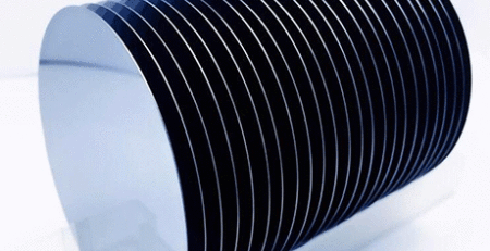
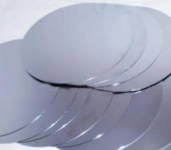
- Silicon wafer, also known as silicon wafer, is the most important basic material for manufacturing semiconductor chips, and its main raw material is monocrystalline silicon.
- A silicon wafer is a sheet-like object made of silicon, generally made of high-purity crystalline silicon. Compared with other materials, the molecular structure of crystalline silicon is very stable, with few free electrons.
- A semiconductor device is a product with a specific conductivity that is finally obtained by changing the molecular structure of silicon by means of photolithography, ion implantation and other means to improve its conductivity.
二, Semiconductor wafer classification
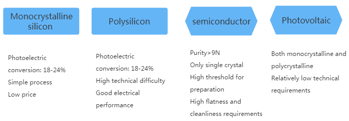
- Semiconductor silicon wafers account for about 37% of the semiconductor manufacturing material market, ranking first among the three core materials for semiconductor manufacturing. .
- The core difficulty of silicon wafers lies in the high purity requirements, which usually require more than 9N.
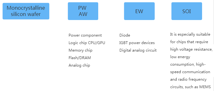
- The wafers used in IC manufacturing are all monocrystalline silicon wafers, and the specific silicon wafer specifications can be divided into three categories: polished wafers PW/AW, epitaxial wafers EW and silicon-on-insulator SOI.
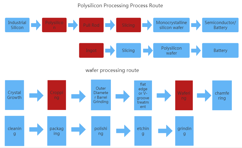
三, Silicon wafer production process
- From the perspective of the production process flow, the preparation of polysilicon, the ingot of silicon material, the pulling rod and the cutting of silicon wafers are the four core technologies in the current silicon wafer production process.
- The process mainly affects the purity, impurity content, compactness, grain size and size distribution, crystal orientation and structure uniformity of the silicon wafer, and the thickness of the silicon wafer.