Photovoltaic silicon wafer cutting
Wafer cutting technology is of great significance in photovoltaic cell materials.Silicon wafers are at the forefront of the manufacturing process in the photovoltaic industry chain.
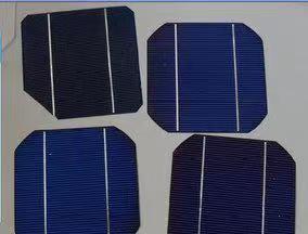
The function of the silicon wafer link is to process the silicon material into silicon wafers of standard size, which are applied to downstream cells and components, and play a role in the industry chain.
At present, in the solar photovoltaic industry, it is usually necessary to process and cut the silicon rod material to obtain a silicon wafer of a predetermined thickness, and then perform a series of processing on the silicon wafer to obtain a finished silicon wafer. This process is more important.
Silicon wafer cutting technology is mainly divided into inner circle cutting and wire cutting technology.
At present, the silicon wafer cutting technology mostly adopts wire cutting technology.
Compared with the previous inner circle cutting, it has the advantages of high cutting efficiency, low cost and less material loss.
Therefore, wire cutting technology is the mainstream of cutting technology in the future.
Among the wire cutting technology, the most prominent is the diamond wire loop cutting.
General speaking, it is an extremely fast closed wire with sharp diamonds on the wire for cutting.
Usually, it is very suitable to cut silicon material with diamond wire with diameter of 0.65mm or 0.5mm.
Below is the video of our cutting silicon material:
https://www.youtube.com/watch?v=N57A-9mi-Mk
Contact us to know more !
and here are more interesting applications .