
Classification of semiconductor silicon wafers according to different parameters
Classification based on different parameters:
Semiconductor Silicon Wafer is the basis for manufacturing silicon semiconductor products
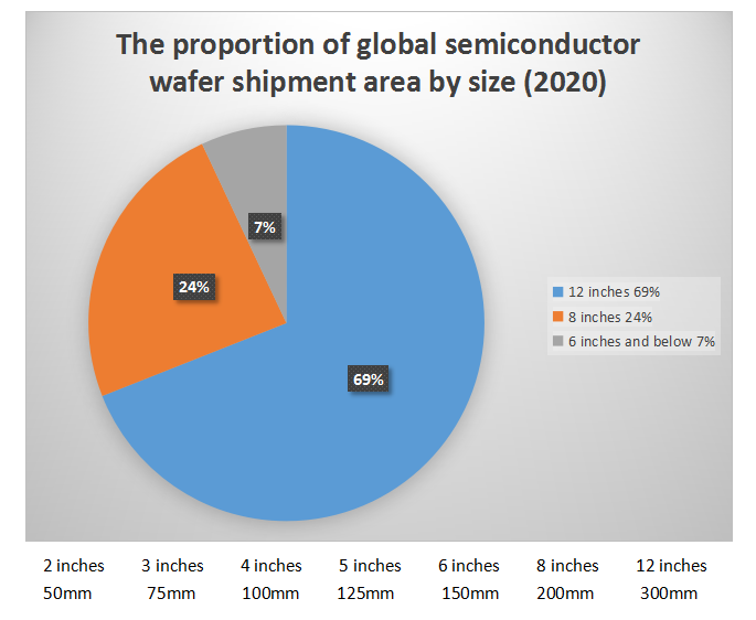
According to different sizes (diameters), semiconductor silicon wafers can be divided into 2 inches (50mm), 3 inches (75mm), 4 inches (100mm), 5 inches (125mm), 6 inches (150mm), 8 inches (200mm), 12 inches Inch (300mm), under the influence of Moore’s Law, semiconductor silicon wafers are constantly developing in the direction of large size. Currently, 8 inches and 12 inches are mainstream products, accounting for more than 90% of the total shipment area.
Classified according to doping level:
According to the degree of doping, semiconductor silicon wafers can be divided into lightly doped and heavily doped.
- Heavy-doped silicon wafers have a large amount of doping elements and low resistivity, and are generally used in power devices and other products;
- Light-doped silicon wafers have a low doping concentration and are generally used in the field of integrated circuits, with higher technical difficulty and product quality requirements.
Since integrated circuits account for more than 80% of the global semiconductor market, there is a greater global demand for lightly doped silicon wafers.
Classification according to process:
According to the process, semiconductor silicon wafers can be divided into grinding wafers, polishing wafers, special wafer epitaxial wafers based on polishing wafers, SOI, etc.
- Grinding sheets can be used to manufacture discrete devices;
- Lightly doped polishing sheets can be used to manufacture large scale integrated circuits or as substrate materials for epitaxial wafers, and heavily doped polishing sheets are generally used as substrate materials for epitaxial wafers.
- Compared with abrasive sheets, polishing sheets have better surface flatness and cleanliness.
- On the basis of polished wafers, annealed wafers, epitaxial wafers, SOI wafers and junction isolation wafers can be fabricated.Annealing wafers High temperature heat treatment of polished wafers in a hydrogen or argon atmosphere to remove oxygen near the wafer surface can improve the integrity of the surface crystals.
- Epitaxial wafer is a layer of vapor-grown single crystal silicon formed on the surface of the polished wafer, which can meet the needs of multi-layer structures that require crystal integrity or different resistivity.
- SOI silicon wafer (Silicon-On-Insulator) is a high electrical insulating oxide film layer inserted between two polished wafers, which can achieve high integration, low power consumption, high speed and high reliability of the device, and can also be used on the surface of the active layer.
A diffusion layer of arsenic or arsenic is formed. Junction isolation silicon wafers are based on customer designs, using exposure, ion implantation and thermal diffusion techniques to pre-form an IC embedded layer on the wafer surface, and then grow an epitaxial layer on top.
Classification according to application scenarios:
According to different application scenarios, semiconductor silicon wafers can be divided into Prime Wafer and Dummy Wafer.
- Prime Wafer is used in the manufacture of semiconductor products, and Dummy Wafer is used to warm up, fill vacancies, and test the process status of production equipment or the quality of a process.
- The dummy wafers are generally cut from the poor quality parts on both sides of the crystal rod. Due to the huge amount of use, some products will be recycled and reused if the conditions are met.
- The recycled silicon wafers are called Reclaimed Wafers. According to the data from Guanyan.com, the 65nm process wafer foundry needs to add 6 fake wafers for every 10 positive wafers, and the 28nm and below process needs to add 15-20 fake wafers for every 10 positive wafers.
https://www.youtube.com/watch?v=N57A-9mi-Mk
Contact us to know more !
and here are more interesting applications .
