Introduction to each link of SiC industry chain and its competition pattern(2)
Introduction to SiC industry chain: upstream substrate, midstream epitaxial wafer, downstream devices and applications. The industry chain based on SiC materials mainly includes the preparation of SiC substrate materials, growth of epitaxial layers, device manufacturing and downstream application markets.
The upstream of SiC industry makes substrate materials from raw materials and then epitaxial materials; The midstream includes SiC devices, SiC power semiconductors, and SiC power modules; Downstream applications include 5G communication, new energy vehicles, photovoltaic, semiconductor, rail transit, steel industry, building materials industry, etc.
According to the different electrical properties, SiC substrate can be divided into semi insulating substrate and conductive substrate. SiC substrate is the core of SiC industry chain, and its electrical performance The electrical performance of the substrate determines the function and performance of downstream chips. In order to enable materials to meet the functional requirements of different chips, SiC substrates with different electrical properties need to be prepared.
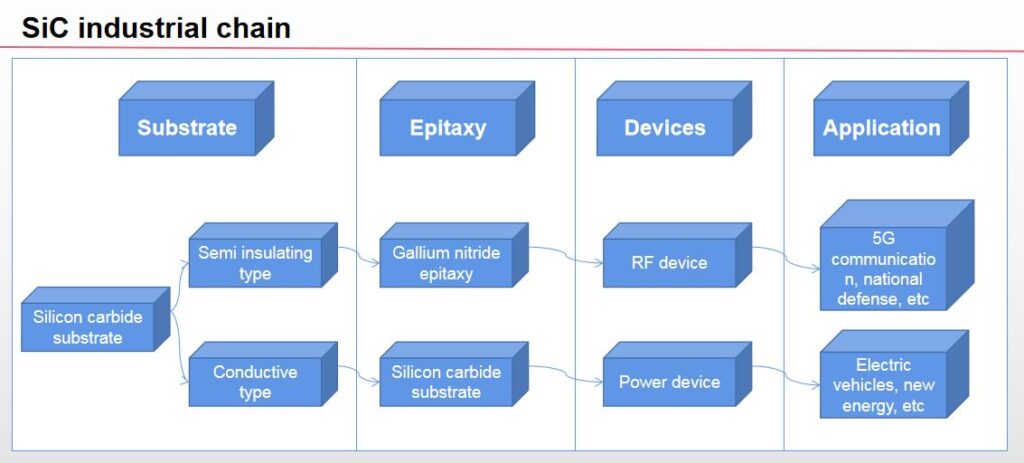
SiC substrate is the cornerstone of GaN and SiC applications in the third generation semiconductor materials. On SiC substrate, chemical vapor deposition (CVD) is mainly used to generate the required thin film materials on the substrate surface, that is, to form epitaxial wafers and further to make devices.
Among them, SiC epitaxial films are made by growing SiC epitaxial layers on conductive SiC substrates, which can further make success rate devices and be used in new energy vehicles, photovoltaic power generation, rail transit, smart grid, aerospace and other fields; GaN on SiC epitaxial wafers are prepared by growing GaN epitaxial layers on semi insulating SiC substrates, which can be further made into microwave RF devices and used in 5G communications, radar and other fields.
Epitaxial sheet refers to one or more epitaxial layers grown on SiC substrate. Compared with the substrate, the epitaxial material has good uniformity in thickness and doping concentration, excellent inter chip consistency, and low defect rate, which effectively improves the consistency and yield of downstream products. Power devices generally require high defect density, high voltage and current tolerance, so epitaxial chips are used for chip manufacturing.
Epitaxial wafers are of great significance for improving the parameter stability of devices. From the perspective of production process, chemical vapor deposition (CVD) is currently the common epitaxial process, that is, epitaxial layers are grown on SiC polished wafers by using an epitaxial furnace and precursor gas. The core technology in epitaxy includes the accurate control of epitaxial temperature, gas flow, time and other parameters, so as to reduce the defect degree of the epitaxial layer and improve the performance and reliability of the device. The epitaxial parameters required by different device designs are also different.
Generally speaking, the thicker the epitaxial layer is, the higher the voltage the device can withstand. For 600V~6500V applications, the thickness of SiC epitaxial layer is generally 1~40 μ m。 Because SiC epitaxy is difficult, there are some manufacturers specialized in SiC epitaxy in the market, such as Hantiancheng, Dongguan Tianyu, etc. At present, domestic 6-inch SiC epitaxial products have been commercialized, and 8-inch products are under development.
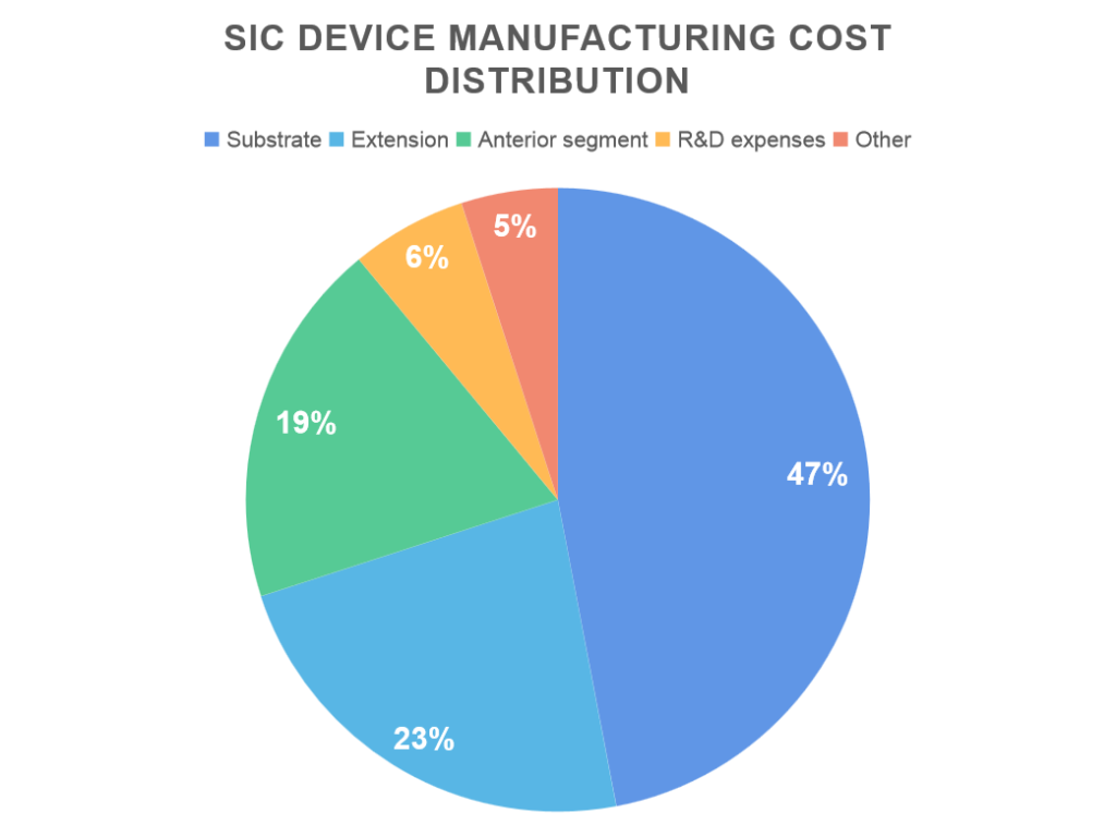
The added value of SiC industry chain is concentrated upstream, and the substrate and epitaxial film are important components of SiC devices. The SiC industry chain from upstream to downstream includes SiC substrate, epitaxial wafer production, device manufacturing, package testing and other links. The substrate is at the top of the SiC industry chain, accounting for 47% of the cost, followed by epitaxial wafer, accounting for 23%.
These two processes are important components of SiC devices. Due to the high technological barriers and low yield of SiC substrate production, the global production has obvious bottlenecks, so its manufacturing cost has been high. In addition, the parameter performance of epitaxial wafers will be affected by the quality of SiC substrate, which will also affect the performance of downstream devices. It can be seen that SiC substrates and epitaxial wafers are the core links of the SiC industry chain, and the added value of the industry is concentrated upstream.
Competition pattern: monopoly of international enterprises
Industry pattern: SiC substrate market is dominated by international enterprises. SiC substrate is a link with high technical barriers in the SiC industry chain, which involves many links such as equipment development and production, raw material synthesis, crystal growth and cutting, wafer processing and cleaning detection. Therefore, long-term process technology accumulation is required, and there are high technical and talent barriers. At present, the SiC substrate market is dominated by international manufacturers. In the first half of 2020, Wolfspeed’s market share in the global SiC substrate market (including semi insulating and conductive types) is up to 45%.
Conductive SiC substrate: According to Yole data, Wolfspeed in the United States is the largest, accounting for more than 60% of the global market share, basically controlling the market price and market standard of the industry. Other companies in the industry include: II-VI in the United States, Si Crystal in Germany, Dow, ShowaDenko in Japan, etc. The top three enterprises account for more than 90% of the industry. Semi insulating SiC substrate: The global market Wolfspeed, II-IV, in the United States, accounts for nearly 70% of the market share in total. The domestic share of Shandong Tianyue is leading in the share of semi insulating SiC substrate, accounting for 30% in 2020.
SiC extension equipment: the market is monopolized by four international enterprises. At present, the global SiC epitaxial equipment is monopolized by the four leading enterprises in the industry, Axitron, LPE, TEL and Nuflare. The market share of the top four enterprises in the industry is close to 100%. At present, the SiC epitaxial equipment of the four major enterprises in the world have their own advantages. Axitron has the strongest epitaxial equipment growth capacity, so its capacity is relatively larger; LPE epitaxial equipment has the highest growth rate; The equipment of Japanese TEL is double chamber, which helps to increase the output; Nuflare has a higher rotation rate of 1000 revolutions per minute, so the product has a stronger uniformity.
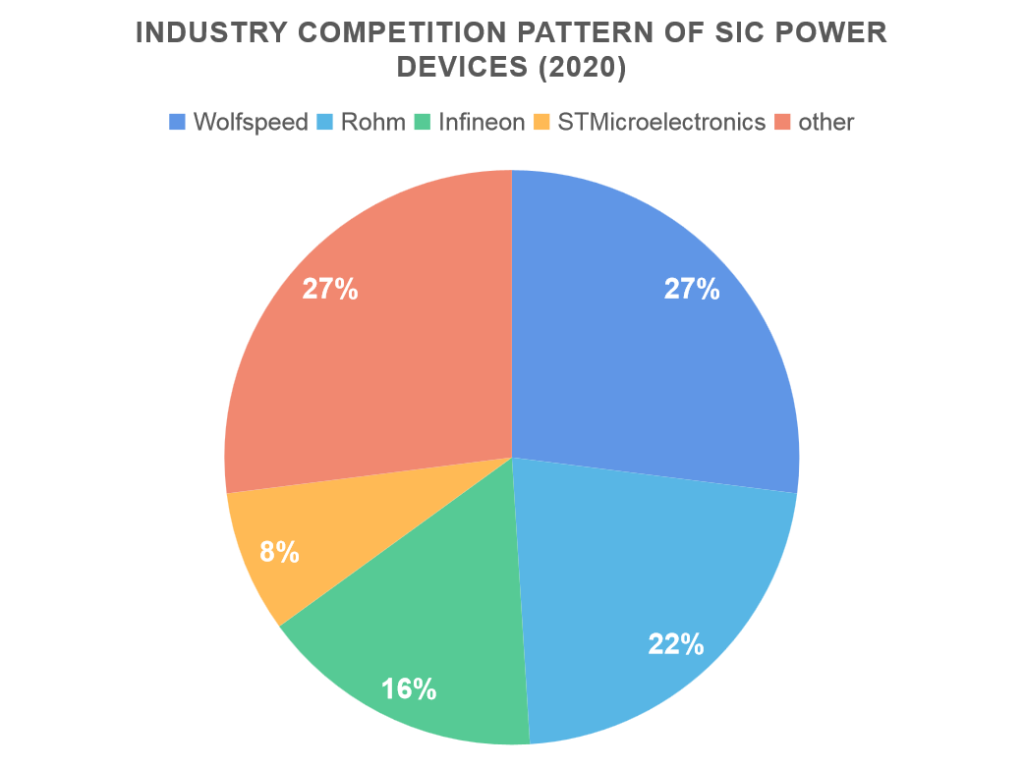
SiC power devices: In the downstream SiC power device field, the world’s main market shares are held by two leading enterprises, Wolfspeed in the United States and Rohm in Japan, with market shares of 27% and 22% respectively. The market share of the top four enterprises in the industry totals 73%. From the perspective of the application of SiC power devices, since SiC power devices can significantly improve the performance of new energy vehicles, such as improving the endurance and charging rate, and realizing the lightweight of vehicles, SiC power devices have the highest proportion of applications in the field of new energy vehicles, followed by power supply equipment, photovoltaic power generation and national defense and military industry, accounting for 21%, 17% and 11% respectively.