Diamond wire cutting is the best choice for cutting hard and brittle materials
Taking the photovoltaic industry as the cornerstone, diamond wire cutting strives to become the world’s leading cutting equipment for high-hardness and brittle materials
Zhengzhou Element Tool Technology Co., Ltd. is currently an industry-leading manufacturer of cutting equipment and consumables for high-hardness and brittle materials. It also has the research and development, production and sales capabilities of cutting equipment and cutting consumables.
The main application scenarios of Ensoll cutting equipment and cutting consumables include photovoltaic industry, magnetic material industry, sapphire industry and semiconductor industry.
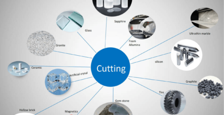
Photovoltaic silicon materials, semiconductor silicon materials, sapphire materials, magnetic materials, optical glass, ceramic materials, etc., all have common characteristics such as wear resistance, high hardness, and high brittleness, and can be collectively referred to as high hardness and brittle materials.
From the perspective of development history, the cutting method of high-hardness and brittle materials has gone through the technical upgrading route of internal circular saw cutting, free abrasive mortar cutting, and diamond wire cutting. Each step of improvement leads to increased raw material utilization, improved cutting efficiency and reduced cutting costs.
In recent years, due to the many disadvantages of free abrasive wire saw cutting, it is gradually replaced by diamond wire cutting.
Compared with traditional cutting, annular diamond wire cutting has the advantages of higher wire speed, more cutting edges, smaller kerf, and can cut any material, with high cutting efficiency, low cost and less material loss.
The replacement of traditional mortar cutting technology by diamond wire cutting technology is advancing rapidly.
The diamond wire cutting technology has taken the lead in completing the large-scale application in the field of photovoltaic silicon material cutting, which has promoted the process of improving the quality and efficiency of the photovoltaic industry and making it affordable to the Internet.
In the field of semiconductor silicon material cutting, diamond wire cutting is also being gradually promoted and applied. In the field of sapphire material and magnetic material cutting, diamond wire cutting has also become an important cutting method.
The photovoltaic industry chain includes five links: silicon materials, silicon wafers, photovoltaic cells, photovoltaic modules, and photovoltaic power generation systems.
The cutting of silicon rods and silicon wafers is the main process in the production of silicon wafers. Cutting technology will directly affect the quality of silicon wafers and the manufacturing cost of photovoltaic modules.
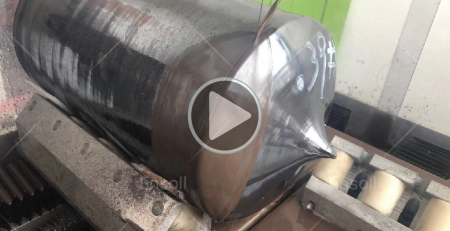
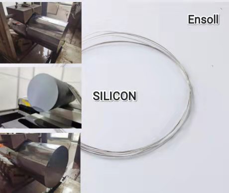
For the moment, Ensoll’s photovoltaic cutting equipment is a diamond wire slicer. Photovoltaic cutting consumables refer to electroplated diamond wire (referred to as “diamond wire”), which is a linear superhard material cutting tool.
Ensoll mass-produces 0.65mm diameter diamond wire products. New diamond wire products with thinner diameters of 0.5mm and 0.35mm have also been successfully developed and launched in mass production. By using Ensoll’s thin-line cutting equipment and consumables products, customers can continue to reduce kerf silicon loss and improve wafer yield.
https://www.youtube.com/watch?v=N57A-9mi-Mk
According to the International Semiconductor Equipment and Materials Association (SEMI) data, for semiconductor manufacturers, silicon wafers account for the largest cost, accounting for 32%.
The purity requirements of semiconductor silicon wafers for polysilicon materials are much higher than that of photovoltaic silicon wafers; the manufacturing difficulty of semiconductor silicon wafers is also greater than that of photovoltaic silicon wafers, and the manufacturing difficulty increases with the expansion of the diameter of silicon wafers.
The chip manufacturing process in the semiconductor industry mainly uses precision equipment to fine-tune monocrystalline silicon wafers, which are the basis of semiconductor products.
From the perspective of semiconductor silicon wafer cutting technology, free abrasive mortar cutting technology is mainly used at present.
Since semiconductor silicon wafers have extremely high requirements on product quality and consistency, and the preparation difficulty is far greater than that of photovoltaic silicon wafers, free abrasive mortar cutting technology is still widely used as a mature and stable technical solution.
The new generation of diamond wire cutting technology is still in the promotion stage in the field of semiconductor wafer manufacturing.
However, referring to the application experience of diamond wire cutting technology in the field of photovoltaic silicon wafer manufacturing, once diamond wire cutting technology realizes large-scale application in semiconductor silicon wafer manufacturing in the future, the market size of diamond wire cutting technology will be greatly increased.
Due to the long industrial chain of the semiconductor wafer industry, the quality control is extremely strict and there are high technical barriers. As the investment and expansion of silicon wafers continue to grow, the market demand for semiconductor wafer cutting equipment and related consumables will also usher in important opportunities.