Semiconductor silicon wafer industry analysis
In recent years, the semiconductor market has performed well due to the gradually strong demand for parts brought about by the construction of telecommunications infrastructure, the continuous increase in the penetration rate of distance education and 5G mobile phones, and the emergence of emerging industries such as communications and automotive semiconductor industries.
The two core pillars of the semiconductor industry are materials and equipment. As an industry of tens of billions of dollars, the market size of semiconductor raw materials is not very large, but there are many kinds of internal materials, the market size of a single product is small, the technical requirements are high, and the differences between sub-industries are large.
The upstream material supply in the semiconductor industry structure mainly includes silicon wafers, electronic gases, photomasks, photoresist supporting chemicals, polishing materials, photoresists, wet chemicals and sputtering targets.
Semiconductor silicon wafers account for 36.6% of the semiconductor material market sales, accounting for the highest proportion, and it is the most important link in the procurement of materials for fabs.
Semiconductor wafers: providing support for the development of the semiconductor industry
Semiconductor silicon wafer refers to a thin slice cut from a silicon single crystal ingot, also known as a silicon wafer. As the core basic product of the semiconductor industry, it provides fundamental support for the development of the industry.
Silicon wafers are round wafers, generally differentiated by diameter, ranging from 50.8mm to 450mm, usually called 6-inch wafers, 8-inch wafers (200mm), 12-inch wafers (300mm), 18-inch wafers (450mm) .
The production efficiency and cost of semiconductors are directly related to wafer size. The larger the wafer size, the higher the number of wafers that can be produced, the higher the production efficiency for the production of semiconductors, the lower the unit consumption of raw materials, and the lower the manufacturing cost.
Driven by Moore’s Law, the mainstream was 4-inch silicon wafers in the 1980s, 6-inch silicon wafers in the 1990s, and 8-inch silicon wafers in the 2000s. At present, the most mainstream products in the global semiconductor wafer market are 12-inch and 8-inch silicon wafers.
In 2020, the market shares of 12-inch silicon wafers and 8-inch silicon wafers are 69.15% and 23.94%, respectively, and the total share of the two sizes of silicon wafers has exceeded 90% for two consecutive years. Equivalent to 8.476 billion square inches (6.24 million pieces/month), 2.934 billion square inches (4.86 million pieces/month) (excluding SOI silicon wafers).
It is estimated that by 2022, the global shipment area of 12-inch semiconductor silicon wafers will exceed 9 billion square feet, and the market share will be close to 70%. 12-inch silicon wafers are mainly used to produce logic, memory chips, etc., and 3DNAND has become the biggest factor for downstream demand growth.
SUMCO’s guidance on the volume and price of silicon wafers, in terms of volume, demand for 12-inch logic silicon wafers is strong, and supply is still tight, DRAM silicon wafer demand recovers and storage-related silicon wafer inventories are close to an appropriate level, and NAND is showing a recovery trend after DRAM.
12-inch silicon wafer shipment trends:
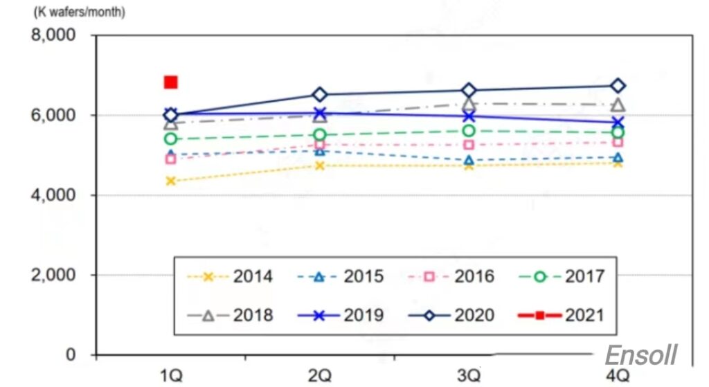
Source: SUMCO
The 8-inch silicon wafer has a mature special process and is mainly used for the production of low-end semiconductor products such as analog ICs, power discrete devices, logic ICs, MCUs, display driver ICs, and CIS image sensors. The terminal application areas are mainly mobile communications, automotive electronics, Internet of Things, industrial electronics, etc., and the demand will maintain steady growth in the future.
Benefiting from the strong demand in application fields such as automotive electronics, industrial electronics and the Internet of Things, the corresponding power devices and sensors are in strong demand, making the 8-inch wafer fab in a state of full production since the end of 2017.
SUMCO pointed out that with the recovery of automotive, consumer and supply demand, strong demand for 8-inch silicon wafers is likely to continue for a long time.
6-inch silicon wafers are mainly concentrated in the field of relatively low-end power devices such as thyristors, rectifier bridges, and cathode tubes. Due to factors such as long product certification cycle and slow product iteration, many automotive semiconductor products are still in the 6-inch production line, but will be gradually upgraded to 8-inch products in the future.
There is huge space for import substitution of semiconductor silicon wafers
According to the statistics of the International Semiconductor Industry Association (SEMI), from 2018 to 2020, the global semiconductor wafer shipment area was 12,541 million square inches, 11,677 million square inches and 12,258 million square inches, respectively. The global semiconductor wafer shipment area is stable at a high level.
In the first quarter of 2021, the global silicon wafer shipment area was 3,337 million square inches, an increase of 4% month-on-month and a year-on-year increase of 14%. The high prosperity of the wafer shipment area verification industry continued.
The fluctuation of the semiconductor wafer market is basically synchronized with the entire semiconductor industry, with a cyclical upward development trend.
The global silicon wafer industry is mainly monopolized by Japan’s Shin-Etsu Chemical, Japan’s SUMCO, Germany’s Siltronic, Taiwan’s Universal Wafer, and South Korea’s SKSiltron, with a market share of 28%, 24%, 14%, 16%, and 10%.