Applications of “Crystal Materials“
Crystal can realize the interaction and conversion of electricity, magnetism, light, sound and force, etc. It is an indispensable and important material in the development of modern science and technology. The need for the development of science and technology has thus promoted the development of intraocular lenses.
Especially due to the rapid development of solid-state microelectronics, a large variety of crystal materials are needed, including semiconductor crystals, laser crystals, scintillation crystals, optical crystals, superhard crystals, insulating crystals and piezoelectric crystals.
The frontier of material science development is closely related to new technologies such as space, electronics, lasers, new energy development, and biomedicine. The types and applications of crystal materials are extremely wide. The following will briefly introduce some common crystal materials and their application scope.
Semiconductor crystals are the main basic raw materials for the semiconductor industry. From the perspective of the breadth and importance of applications, it occupies the first and most important position in crystalline materials.
Semiconductor crystals have been developed since the 1950s. The first generation of semiconductor representative materials: germanium (Ge) single crystals and silicon single crystals (Si), which are made of various diodes, triodes, field effect transistors, SCR and high-power tube, etc.
The rapid development of integrated circuits from only a dozen unit circuits to ultra-large-scale integrated circuits containing thousands of components has triggered the rapid development of the microelectronics field with integrated circuits (ICs) as the core, and greatly improved the work of integrated circuits. At the same time, the cost is reduced. This in turn promotes the wide application of integrated circuits in space research, nuclear weapons, missiles, radar, electronic computers, military communication equipment and civilian use.
The second-generation semiconductor materials are compound semiconductors based on gallium arsenide (GaAs), indium antimonide (InSb), and indium phosphide (InP), which are mainly used to make high-frequency, high-speed and high-power electronic devices.
It is widely used in satellite communication, mobile communication and optical communication. GaAs and indium phosphide semiconductor lasers have become key devices in optical communication systems, and GaAs high-speed devices have also opened up new industries for optical fibers and mobile communications.
The raw materials of GaAs, InP and other compound materials are scarce and need to be formed through synthesis. The price is relatively high, and they are more harmful to the environment, making them difficult to be widely used and limited, and gradually replaced by third-generation semiconductor materials.
The third-generation semiconductor materials are mainly wide-bandgap semiconductor materials represented by silicon carbide (SiC), gallium nitride (GaN), zinc oxide (ZnO), diamond, and aluminum nitride (AlN).
Compared with the first and second generation semiconductor materials, the third generation semiconductor materials have a wide band gap, high breakdown electric field, high thermal conductivity, high electron saturation rate and higher radiation resistance.
Therefore, it is more suitable for making high-temperature, high-frequency, radiation-resistant and high-power devices, and is often referred to as a wide-bandgap semiconductor material (gap width greater than 2.2ev), also known as a high-temperature semiconductor material.
Generally, gallium nitride, silicon carbide and other materials are called wide bandgap semiconductors; gallium nitride, aluminum nitride, indium nitride and their mixed crystal materials are called nitride semiconductors, or gallium nitride, gallium arsenide, Indium phosphide is called a III-V semiconductor.
02. Optical crystal
Optical crystals are crystals used as optical components, such as halide crystals lithium fluoride, calcium fluoride, magnesium fluoride, barium fluoride, they have good transmission characteristics in ultraviolet and infrared, so they can be used as ultraviolet excimer Output windows for lasers and some IR lasers, lenses, prisms, polarizers, waveplates, etc.
Oxides such as sapphire Al2O3, yttrium vanadate YVO4, crystal, etc. It can also be used as the working windows of the above lasers, optical isolators, circulators, beam splitters and optical polarizers.
Semiconductor single crystal silicon, germanium, selenium, gallium arsenide and zinc selenide, zinc sulfide have good transmission performance in far infrared, and can be used as carbon dioxide laser (output window, lens, prism, etc.)
03. Laser crystal
Laser is a wonderful “substance”, and it is another great discovery of mankind after atomic energy, computer and semiconductor. Everyone knows that the brightness of the laser is extremely high, which can reach 1 billion times the brightness of the sun or even higher;
The laser is extremely pure and has excellent monochromaticity; the laser has unparalleled collimation (straight line propagation); Instant bursts of energy that can penetrate and melt even the hardest objects. Therefore, laser is widely used in production, life and scientific research, and it is a powerful weapon for people to explore nature.
A device that produces a laser is called a laser. Among the current various lasers, all-solid-state lasers are the most promising. Laser crystal, which can convert the energy provided by the outside world through an optical resonator into a highly parallel and monochromatic laser crystal material coherent in space and time. Basic supporting materials for the industry.
Common laser crystal materials include neodymium-doped yttrium aluminum garnet crystal Nd:YAG, neodymium-doped yttrium vanadate crystal Nd:YVO4, neodymium-doped lithium yttrium fluoride crystal Nd:YLF, titanium sapphire crystal, ruby crystal, etc.
04. Scintillation crystal
Under the impact of high-energy particles, the crystals that can convert the kinetic energy of high-energy particles into light energy and emit fluorescence are called scintillation crystals. Scintillation crystals can be used for the detection of x-rays, gamma rays, neutrons and other high-energy particles.
The detection and imaging technology centered on scintillation crystals has been widely used in nuclear medicine, high-energy physics, safety inspection, industrial non-destructive testing, space physics and nuclear prospecting.
The commonly used scintillation crystal materials are cultivated by artificial methods, and there are many kinds. At present, the most used scintillation crystals are BGO (abbreviation of bismuth germanate, the general name of Bi2O3-GeO2 series compounds), CsI (cesium iodide), PbWO4 (lead tungstate) and so on.
05. Super hard crystal
Diamond, also known as “diamond”, is a natural mineral and the hardest substance known to exist in nature. Elemental crystal. The diamonds that can be found and mined in nature are extremely rare. Usually, fine diamonds with a total weight of 1 carat can be obtained in every 4 cubic meters of rich ore. Crystal clear, flawless large-sized diamonds are even rarer.
Since the 1950s, people have researched and developed a variety of synthetic diamond methods, mainly including high temperature and high pressure (HTHP), chemical vapor deposition (CVD), and detonation. In 1955, GE used the high temperature and high pressure method to synthesize diamond crystals for the first time.
In the 1980s, the world set off an upsurge in CVD diamond research, and developed various preparation methods such as hot wire method (HFCVD), microwave plasma (MPCVD) and DC arc plasma jet CVD, which laid the foundation for later applications.
High hardness is one of the many characteristics of diamond. Using the extremely high hardness of diamond, it can be prepared into various tools, which play an irreplaceable role in processing stone, non-ferrous metals, and difficult-to-machine composite materials (such as carbon fiber composite materials). To achieve efficient, high-precision, environmentally friendly processing.
When it comes to diamond, it can be linked to a new type of superhard material cubic boron nitride crystal, cubic boron nitride-CBN, its crystal structure is similar to diamond, its hardness is slightly lower than diamond, but its thermal stability is much higher than diamond , has greater chemical stability to iron-based metal elements.
The grinding performance of cubic boron nitride abrasives is very good, not only can it be competent for the processing of difficult-to-grind materials, but also improve productivity, chemical inertness, and can effectively improve the grinding quality of workpieces.
06. Piezoelectric crystal material
When the crystal is subjected to external force, the crystal will polarize and form surface charge, which is called the positive piezoelectric effect; Conversely, when the crystal is subjected to an external electric field, the crystal will deform, which is called the inverse piezoelectric effect. Crystals with piezoelectric effect are called piezoelectric crystals, which only exist in crystals without a center of symmetry.
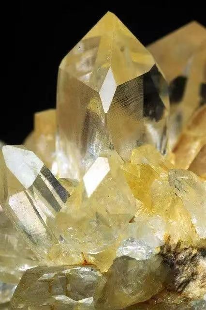
The earliest discovered piezoelectric crystal is crystal (α-SiO2), which has the characteristics of frequency stability and is an ideal piezoelectric material, which can be used to manufacture resonators, filters, transducers, optical deflectors, surface acoustic waves devices and various thermal, gas-sensitive, photosensitive and chemical-sensitive devices, etc. It is also widely used in people’s daily life, such as quartz watches, electronic clocks, color TVs, stereo radios and tape recorders.
In recent years, many new piezoelectric crystals have been developed, such as lithium niobate (LiNbO3) and potassium niobate (KNbO3) with perovskite structure. Using the piezoelectric effect of these crystals, various devices can be made, which are widely used in military and civilian industries, such as sphygmomanometers, piezoelectric keyboards, delay lines, oscillators, ultrasonic transducers, piezoelectric transformers, etc.
07. Insulating crystal
A typical example of insulating wafers is mica wafers. Mica is a general term for layered silicate minerals. It has the characteristics of insulation, transparency, heat resistance, corrosion resistance, easy peeling and elasticity. It is widely used in motors, electrical appliances, electronics, radios and household appliances.
It plays an important role in economic and national defense construction. Although there are many types of natural mica, the most widely used in industry is muscovite mica, followed by phlogopite mica.
Due to the low reserves of natural mica in many countries, especially high-quality, large-scale mica, which cannot meet the development needs of the electronics industry, synthetic mica has been studied since the 1950s.
Because synthetic mica has excellent properties such as purity, transparency, high temperature resistance, corrosion resistance and electrical insulation, synthetic mica single wafers can be used in:
① Insulating racks in various vacuum devices, such as accelerators, ionization chambers, magnetrons and electron tubes, etc. ;
② Window materials, such as microwave tube output windows, high temperature furnace observation windows and acid and alkali resistant windows;
③ High pressure boiler water level gauges in thermal power plants;
④ High temperature capacitors, platinum wire surface thermometer skeleton, etc.
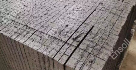
Below the crystal cutting video for reference:
https://www.youtube.com/watch?v=VA3P7tIrT44