Precision Cutting of Bifacial Solar Cell Materials: Why Diamond Cutting Wire Loop Technology Leads the Industry
Introduction to Bifacial Solar Technology
Bifacial solar cells represent one of the most significant advancements in photovoltaic technology, capable of capturing sunlight from both front and rear surfaces to increase energy generation by up to 30% compared to traditional monofacial panels. These sophisticated cells require exceptional manufacturing precision, particularly during the cutting process where material integrity directly impacts performance and longevity.
The unique structure of bifacial cells – featuring transparent rear surfaces and specialized conductive materials – demands cutting technologies that preserve edge quality and minimize micro-damage. While several cutting methods exist, diamond cutting wire loop technology has emerged as the superior solution for manufacturing high-efficiency bifacial solar modules.
Understanding Bifacial Solar Cell Materials
Bifacial technology utilizes several advanced material configurations:
Monocrystalline Silicon with Passivated Contacts
– PERC (Passivated Emitter Rear Cell) structures
– TOPCon (Tunnel Oxide Passivated Contact) designs
– HJT (Heterojunction Technology) configurations
Specialized Transparent Conductive Materials
– Indium Tin Oxide (ITO) layers
– Thin-film transparent conductive oxides
– Advanced anti-reflective coatings
Dual-Surface Architecture
– Symmetrical electrical characteristics
– Enhanced light trapping structures
– Thinner wafers (120-160μm) for improved bifaciality
The sophisticated structure of bifacial cells creates unique cutting challenges:
Edge Quality Requirements
– Mirror-like edge finish necessary for optimal light capture
– Minimal micro-cracks to prevent efficiency degradation
– Precise dimensional tolerances (±0.1mm) for automated assembly
Material Sensitivity Issues
– Brittle silicon wafers prone to chipping and cracking
– Delamination risk for thin-film conductive layers
– Thermal sensitivity of passivation layers
Production Efficiency Demands
– High-volume manufacturing requirements
– Consistent quality across thousands of wafers
– Rapid processing without sacrificing precision
Why Diamond Cutting Wire Loop Technology Excels
Superior Cutting Performance
Minimal Kerf Loss
Diamond cutting wire loop technology achieves exceptional material conservation with kerf widths of 80-120μm, significantly less than traditional abrasive methods (180-250μm) and comparable to laser cutting but without thermal damage. This precision is particularly valuable for expensive bifacial cell materials.
Exceptional Edge Quality
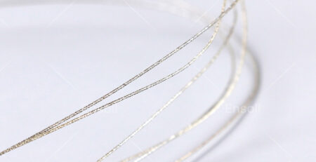
The continuous loop system with diamond-embedded wires produces edges with surface roughness below 0.3μm, essential for maintaining the optical properties of bifacial cells. This smooth finish minimizes light scattering and maximizes energy capture from both surfaces.
No Thermal Damage
Unlike laser cutting which creates heat-affected zones (HAZ) that degrade cell performance, diamond wire looping operates at ambient temperature, preserving the electrical properties of sensitive passivation layers and transparent conductive materials.
Production Efficiency Advantages
High Throughput Capability
Modern diamond wire loop systems process 2,000-3,000 wafers per hour, significantly outperforming laser systems (800-1,200 wafers/hour) while maintaining superior quality consistency.
Reduced Downtime
Advanced tension control systems and automated wire threading minimize changeover time, with typical wire lifespan exceeding 500 kilometers of cutting before replacement.
Scalability
The technology easily scales from pilot production to gigawatt-scale manufacturing, with multi-wire systems capable of processing entire ingots in single operations.
Comparative Analysis: Cutting Technologies for Bifacial Cells
| Parameter | Diamond Wire Loop | Laser Cutting | Ultrasonic Machining |
| Cutting Speed | 15-25 m/s | 5-12 m/s | 2-8 m/s |
| Edge Quality | Excellent (Ra<0.3μm) | Good (Ra 0.8-1.2μm) | Fair (Ra 1.5-2.0μm) |
| Thermal Impact | None | Significant HAZ | Minimal |
| Kerf Loss | 80-120μm | 30-50μm | 150-200μm |
| Operating Cost | $0.03-0.06/wafer | $0.08-0.12/wafer | $0.10-0.15/wafer |
| Yield Impact | +1.5-2.0% efficiency | -0.5-1.0% efficiency | -1.0-1.5% efficiency |
Implementation in Bifacial Cell Production
Process Optimization
Wire Selection Criteria
– Diamond grit size: 15-25μm for optimal cutting speed and finish
– Wire diameter: 100-120μm balancing strength and kerf loss
– Tension control: 15-25N for consistent cutting performance
Coolant Management
– Deionized water with specialized additives
– Temperature control (±1°C) for dimensional stability
– Filtration systems maintaining <1μm particle size
Quality Control Systems
– In-line optical inspection for edge defects
– Automated thickness measurement
– Real-time breakage detection
Performance Results
Manufacturers implementing diamond cutting wire loop technology report:
– 99.8% yield rates for premium bifacial cells
– 1.8% average efficiency gain versus laser-cut cells
– 40% reduction in cutting-related rejections
– 25% lower operating costs compared to laser systems.
Future Trends and Developments
Advanced Wire Technology
– Nanocomposite diamond coatings for extended lifespan
– Smart wires with embedded sensors for real-time monitoring
– Hybrid wires combining cutting and cleaning functions
Integration with Industry 4.0
– AI-powered predictive maintenance
– Digital twin systems for process optimization
– Automated quality classification using machine learning
Sustainability Improvements
– Water recycling systems reducing consumption by 80%
– Wire recycling programs achieving 95% material recovery
– Energy-efficient drives cutting power usage by 40%
Conclusion: Why Diamond Cutting Wire Loop is Essential for Bifacial Success
The transition to bifacial solar technology demands manufacturing processes that match the sophistication of the product. Diamond cutting wire loop technology provides the precision, efficiency, and reliability required for mass production of high-performance bifacial solar cells.
Key advantages include:
– Superior edge quality enhancing optical performance
– Zero thermal damage preserving electrical properties
– High production throughput meeting volume demands
– Excellent cost efficiency improving manufacturing economics