Inside the Fab Wafer: How Raw Crystals Become the Engines of Modern Electronics
Introduction: The Silent Foundation of Everything Electronic
Every computer processor, every memory chip, every sensor in your smartphone, and every power management circuit in your electric vehicle starts as something surprisingly simple: a fab wafer.
The term “fab wafer” combines two ideas. “Fab” is short for fabrication facility—the highly controlled cleanroom where semiconductors are made. “Wafer” refers to the thin, disk-shaped slice of material that serves as the substrate for integrated circuits.
But before a wafer ever enters a fab, it must be created from raw crystal. And one of the most critical steps in that creation process is cutting. This is where the diamond wire saw plays an essential role that few people outside the industry ever see.
This article explains what a fab wafer is, how it is made, and why diamond wire saw technology has become the standard method for transforming crystals into wafers.
What Exactly Is a Fab Wafer?
A fab wafer is a thin, circular slice of ultra-pure semiconductor material. Most commonly, that material is silicon, although other materials like gallium arsenide or silicon carbide are used for specialized applications.
The wafer serves two main purposes inside a fabrication facility:
First, it provides a physically stable platform. Semiconductor devices are incredibly small—measured in nanometers. They cannot be built on flexible or uneven surfaces. The wafer offers a flat, rigid foundation.
Second, it provides the electrical properties needed for device operation. Silicon is a semiconductor, meaning its electrical conductivity can be precisely controlled by adding tiny amounts of other elements (doping). This allows transistors, diodes, and other components to be created directly in the wafer material itself.
Fab wafers come in standard diameters. The industry has moved from 1-inch and 2-inch wafers in the early days to 4-inch, 6-inch, and now predominantly 8-inch (200mm) and 12-inch (300mm) wafers. Larger wafers allow more chips to be produced from each wafer, reducing cost per device.
From Sand to Crystal: The Starting Point
Before there is a wafer, there is raw material. For silicon wafers, the starting point is quartzite—a high-purity form of quartz sand. This quartz is refined into polysilicon, then melted and re-crystallized into a single large crystal ingot.
The most common method is the Czochralski (CZ) process. A small seed crystal is dipped into molten silicon and slowly pulled upward while rotating. As the seed lifts, silicon solidifies around it, forming a cylindrical single crystal. These ingots can weigh hundreds of kilograms and measure 300mm or more in diameter.
For other materials like gallium arsenide or indium phosphide, similar crystal growth methods are used, but the equipment and conditions differ because these materials have different melting points and chemical behaviors.
The Critical Cut: How Diamond Wire Saw Enters the Process
Once a crystal ingot is grown, it must be sliced into individual wafers. This is where the diamond wire saw becomes the central tool.
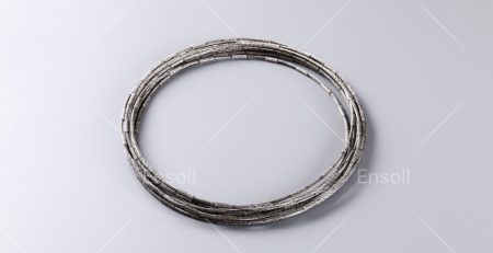
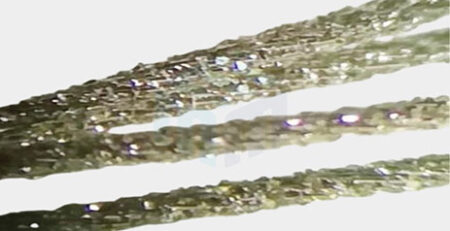
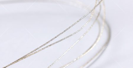
A diamond wire saw consists of a thin steel wire coated with diamond abrasive particles. The wire is formed into a continuous loop or spooled between reels. As the wire moves at high speed, it presses against the crystal ingot, grinding away material along the cut line.
Why diamond wire saw instead of older methods?
In the early days of semiconductor manufacturing, wafers were cut using inner-diameter (ID) saws—circular blades with diamond grit on their inner edge. ID saws worked, but they had major drawbacks.
First, ID blades had a thick kerf—the width of material removed during cutting. A thick kerf meant significant material loss. When a single silicon ingot costs thousands of dollars, lost material directly reduces profit.
Second, ID saws introduced mechanical stress and vibration into the crystal. This caused subsurface damage that required thicker wafers to survive后续 processing.
Third, ID saws struggled with larger diameter ingots. As the industry moved from 6-inch to 8-inch and 12-inch wafers, ID blades became impractical.
Diamond wire saw solved these problems. The wire is much thinner than any blade, resulting in a narrower kerf and less material waste. The continuous, unidirectional motion of the wire reduces vibration and mechanical stress. And because the wire is flexible and can be made very long, diamond wire saws easily handle 12-inch and even larger ingots.
Beyond Silicon: Diamond Wire Saw for Other Fab Wafer Materials
While silicon dominates the semiconductor industry, other materials require fab wafers as well:
– Silicon carbide (SiC) for high-power and high-frequency applications
– Gallium nitride (GaN) for RF and power electronics
– Sapphire for LED and specialty device substrates
– Lithium niobate for optical modulators and RF filters
All of these materials are hard, brittle, and challenging to cut. The diamond wire saw is equally effective on these materials because diamond is the hardest known material. Whether slicing a sapphire boule or a lithium niobate crystal, the diamond wire saw produces clean, low-stress cuts with minimal waste.
From Cut Wafer to Fab-Ready Substrate
After the diamond wire saw completes its cut, the resulting wafer is not yet ready for the fabrication facility. Several processing steps follow:
Lapping removes saw marks and flattens the wafer surface. The wafer is pressed between rotating plates with an abrasive slurry.
Etching removes subsurface damage left by the cutting and lapping processes. Chemical etchants dissolve a thin layer of material, revealing a damage-free surface.
Polishing creates a mirror-like finish. The wafer is pressed against a soft polishing pad with a fine silica slurry. This step produces the smooth, reflective surface that allows photolithography to pattern circuits accurately.
Cleaning removes any remaining particles or chemical residues. Fab wafers must be extraordinarily clean—a single dust particle can ruin dozens of chips.
Finally, the finished wafers are sealed in protective cassettes and shipped to fabrication facilities around the world.
Inside the Fab: What Happens to the Wafer
Once a fab wafer arrives at a semiconductor fabrication plant, it undergoes hundreds of individual processing steps:
– Oxidation grows a thin silicon dioxide layer on the wafer surface
– Photolithography patterns circuit designs using light-sensitive chemicals
– Etching removes material where the pattern allows
– Deposition adds thin films of conductive or insulating materials
– Doping introduces impurities to modify electrical properties
– Metallization creates wiring layers to connect transistors
After weeks of processing, each wafer contains hundreds or thousands of individual chips—processors, memory dies, sensors, or other devices. The wafer is then tested, diced into individual chips, and packaged for use in electronic products.
Why Diamond Wire Saw Matters for Fab Wafers
The quality of a fab wafer begins with the cut. A poorly cut wafer has rough edges, subsurface cracks, and variable thickness. These defects reduce the number of usable chips or cause device failures later in the manufacturing process.
The diamond wire saw delivers cuts that are:
– Consistent – uniform thickness across the entire wafer diameter
– Low-damage – minimal cracking beneath the cut surface
– Material-efficient – narrow kerf saves expensive crystal material
– Scalable – works for 4-inch through 12-inch wafers and beyond
Without diamond wire saw technology, the modern semiconductor industry would either waste far more material or produce wafers of lower quality. Neither outcome is acceptable when chip features are measured in nanometers and fab facilities cost billions of dollars.
Conclusion: The Unseen Tool Behind Every Chip
The next time you use a smartphone, start a car, or boot a computer, consider the journey that made it possible. Somewhere along that journey, a crystal ingot was mounted on a diamond wire saw and sliced into thin, precise wafers. Those wafers traveled to a fabrication facility, where they were transformed into the circuits that power modern life.
The fab wafer is the foundation of the electronics industry. And the diamond wire saw is one of the essential tools that makes that foundation possible. It works silently, reliably, and with remarkable efficiency—turning raw crystals into the substrates that build our digital world.
Whether you are an engineer, a student, or simply someone curious about how things work, understanding the connection between diamond wire saws and fab wafers gives you a deeper appreciation for the precision manufacturing that surrounds us every day.