Diamond Wire Cutting: The Key to Perovskite Solar Potential
In the dynamic arena of advanced materials, perovskite structures stand out for their revolutionary potential, particularly in next-generation photovoltaics where their high conversion efficiency and lower production costs promise a new era for solar energy. However, the very properties that make perovskites remarkable also render them exceptionally challenging to process. Their inherent brittleness and sensitivity to thermal and mechanical stress create a critical bottleneck in manufacturing and R&D. This is where the cold, precise, and gentle nature of Diamond Wire Loop Cutting emerges not merely as an alternative, but as an indispensable enabling technology for the entire perovskite value chain.
The Achilles’ Heel of a Wonder Material: Why Precision Cutting Matters
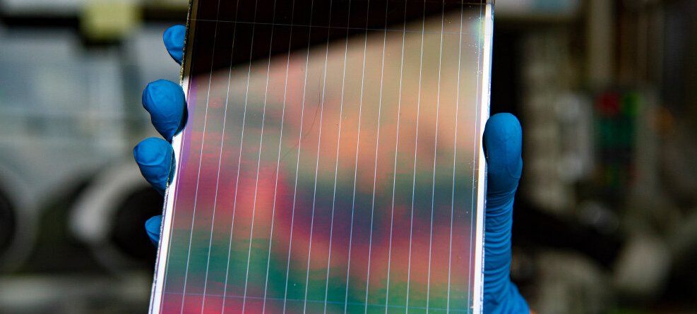
Before delving into the solution, it’s crucial to understand the problem. Perovskite materials, especially in thin-film form for solar cells, are incredibly delicate. The architecture of a perovskite solar cell is a complex, multi-layered stack where each layer—from the transparent conductive oxide substrate to the perovskite absorber layer and the metal electrodes—is often only nanometers to a few microns thick. Any fabrication step, including cutting and dicing, must be performed with surgical precision to avoid catastrophic failures.
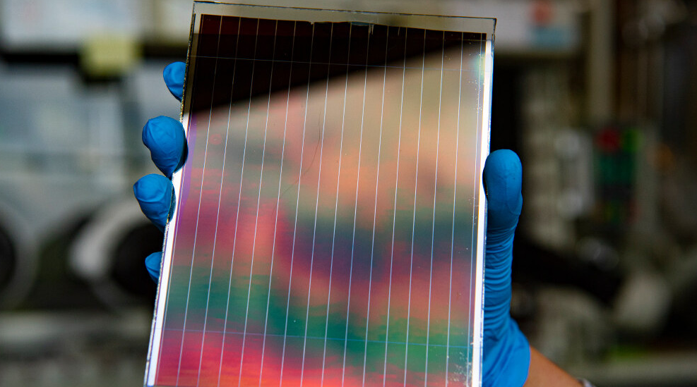
Traditional mechanical cutting methods introduce high lateral forces, causing chipping, cracking, and delamination of these fragile layers. More advanced thermal processes like laser cutting, while precise, come with their own significant drawback: the heat-affected zone (HAZ). The intense, localized heat from a laser beam can alter the crystalline structure of the perovskite, degrade the interfaces between layers, and create micro-cracks that propagate over time. Research has shown that such thermal damage from laser cutting can lead to increased non-radiative recombination at the cut edges, directly lowering the open-circuit voltage and fill factor of the solar cell, thereby reducing its overall power conversion efficiency. For a technology racing toward commercialization, losing even 1% of efficiency at the cutting stage is unacceptable.
The Diamond Wire Advantage: A Paradigm of Cold, Clean Cutting
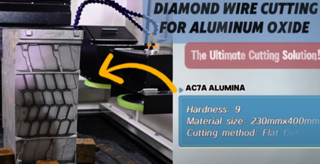
Diamond Wire Loop Cutting, also known as a diamond wire saw, operates on a fundamentally different principle that sidesteps these pitfalls. The technology utilizes a continuous loop of high-tensile steel wire, electroplated with microscopic diamond particles, moving at high speeds. As this wire is drawn across the material, the diamond abrasives perform a micro-grinding action, removing material with minimal force and, most importantly, negligible heat generation.
This “cold cutting” capability is the cornerstone of its advantage for perovskites. The process temperature can remain remarkably low, with studies showing it can be kept below 40°C. This eliminates the thermal damage and heat-affected zones that plague laser methods, preserving the pristine electronic properties of the perovskite material and the integrity of its interfaces.
The benefits extend far beyond temperature control:
Minimal Mechanical Stress and Superior Edge Quality: The cutting force is distributed along the length of the wire and is significantly lower than that of blade-based systems. Advanced systems that incorporate ultrasonic vibration further reduce the average cutting force to just one-third to one-fifth of conventional wire sawing. This results in clean, smooth cut edges with minimal micro-cracks or subsurface damage, which is crucial for maintaining the mechanical strength of thin, brittle samples.
Exceptional Precision and Minimal Material Waste (Kerf Loss): The diamond wire itself can be extremely thin, with diameters ranging from 0.3mm to 3.5mm. This allows for an exceptionally narrow cut, or kerf. When cutting valuable research-grade perovskite crystals or optimizing the active area of a solar panel, minimizing this lost material directly translates to higher yield and lower cost. The cutting precision ensures straight, parallel slices with high dimensional accuracy, which is vital for research reproducibility and device integration.
Versatility Across Material Forms: Whether you are dicing a large-area perovskite-on-glass substrate into smaller cells for testing, sectioning a crystalline perovskite sample for fundamental research, or preparing cross-sectional samples of a complete device stack for electron microscopy analysis, the diamond wire saw is uniquely capable. It can cleanly cut through multi-material composites—such as glass/TCO/perovskite/metal—without causing layer separation or undue damage to any single component.
From Lab to Fab: Applications Enabled by Precision Cutting
The application of diamond wire cutting is transformative across the entire perovskite development lifecycle, from basic research to pilot production.
- Research, Development, and Failure Analysis: In the lab, the primary goal is to understand material properties and device physics. Diamond wire saws are the gold-standard tool for preparing samples. Scientists can use them to create perfectly uniform substrates from bulk crystals, dice pilot devices into controlled sizes for comparative testing, and, most importantly, produce pristine cross-sections of complete solar cells. These flawless cross-sections are essential for advanced microscopy (SEM, TEM) and spectroscopy techniques, allowing researchers to scrutinize layer thickness, interface quality, and identify failure mechanisms without the artifacts introduced by crush damage or thermal alteration.
- Enabling High-Efficiency Tandem Solar Cells: One of the most promising near-term applications for perovskites is in tandem solar cells, where a perovskite cell is stacked on top of a conventional silicon cell to capture a broader spectrum of sunlight. Research from institutions like Ningbo University has directly utilized commercial diamond-wire-sawn silicon wafers as the bottom cell. The texture and roughness of the silicon surface created by the diamond wire cut have been successfully engineered to support the subsequent deposition of high-quality, uniform perovskite films. This synergy has enabled the fabrication of perovskite/silicon tandem cells with certified efficiencies reaching 28%, showcasing how an industrial cutting process directly enables record-breaking laboratory performance.
- Prototyping and Niche Manufacturing: For specialized applications like flexible perovskite solar cells for wearable electronics or custom-shaped cells for building-integrated photovoltaics (BIPV), the flexibility of the diamond wire allows for more complex cutting paths than rigid tools. Its clean, cold process is also ideal for cutting sensitive substrates like polymers or thin metal foils without melting or warping them.
The Future is Cut with Precision
As the perovskite industry progresses from small lab cells to large-area modules and gigawatt-scale manufacturing, the demand for precise, reliable, and damage-free segmentation will only intensify. While laser scribing (P1, P2, P3 lines) will likely remain the dominant technology for monolithic interconnection within a panel, diamond wire loop cutting holds a critical and irreplaceable position in the upstream and downstream processes. It is the enabling technology for substrate preparation, cell isolation, module trimming, and, above all, for the fundamental research that drives the technology forward.
In the quest to commercialize perovskite solar technology, every percentage point of efficiency and every millimeter of yield is fought for. Diamond Wire Loop Cutting provides the essential “cold precision edge,” ensuring that the miraculous properties engineered into perovskite materials in the lab are not lost in the workshop, but are faithfully preserved and delivered into the final device. It is more than a cutting tool; it is a bridge between scientific promise and industrial reality.