
Fab Wafer: From Crystal to Chip
Introduction: The Unsung Hero of the Digital Age
Every time you send a text message, stream a video, or start your car, you are relying on something so small that millions of them can fit on a single fingertip. That something is the integrated circuit, and its foundation is the fab wafer.
The term “fab wafer” combines two essential concepts in semiconductor manufacturing. “Fab” is short for fabrication facility—the ultra-clean factory where chips are born. “Wafer” refers to the thin, disk-shaped slice of semiconductor material that serves as the substrate for all integrated circuits. Together, they represent the starting point of every electronic device that defines modern life.
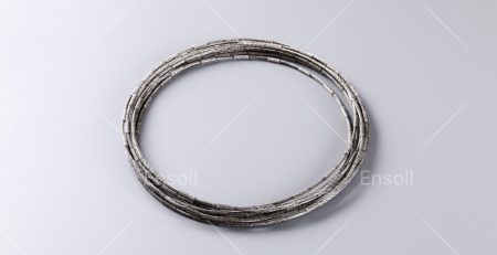
But before a wafer ever enters the fab, it must be created from raw crystal with extraordinary precision. This is where advanced cutting technology enters the story. Ensoll’s diamond wire loop represents the culmination of decades of innovation in precision slicing, offering the consistency and quality that semiconductor manufacturing demands. In this comprehensive guide, we will explore what fab wafers are, how they are made, and why the cutting process matters more than most people realize.
Part One: What Exactly Is a Fab Wafer?
The Basic Definition
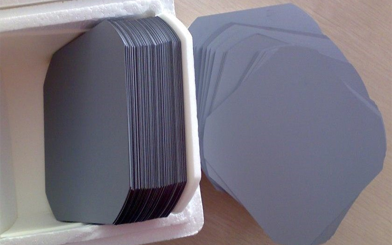
A fab wafer is a thin, circular slice of ultra-pure semiconductor material, typically silicon. These wafers serve as the physical and electrical foundation upon which integrated circuits are built. Think of a wafer as the “real estate” where dozens, hundreds, or even thousands of individual chips will be constructed.
Standard wafer diameters have grown over the decades as manufacturing technology advanced:
| Diameter | Common Name | Era of Adoption |
| 50mm | 2-inch | 1970s |
| 100mm | 4-inch | 1980s |
| 150mm | 6-inch | 1990s |
| 200mm | 8-inch | Late 1990s–2000s |
| 300mm | 12-inch | 2000s–present |
| 450mm | 18-inch | Emerging |
Larger wafers are economically desirable because they allow more chips to be produced from each wafer, reducing the cost per device. However, larger wafers also demand greater precision in every manufacturing step—starting with how the wafer is cut from the crystal ingot.
The Material: Why Silicon?

While several semiconductor materials exist, silicon dominates the industry for compelling reasons:
- Abundance and Cost: Silicon is the second most abundant element in the Earth’s crust (after oxygen). The raw material—common quartz sand—is inexpensive and widely available.
- Semiconductor Properties: Silicon has a bandgap of 1.12 eV at room temperature, making it an ideal semiconductor. It can be “doped” with impurities to precisely control its electrical conductivity.
- Stable Oxide: Silicon dioxide (SiO₂) grows naturally on silicon surfaces and serves as an excellent electrical insulator. This oxide layer is fundamental to MOSFET (Metal-Oxide-Semiconductor Field-Effect Transistor) technology, the building block of nearly all modern digital circuits.
- Mature Manufacturing: Decades of research and development have produced an extensive ecosystem of equipment, processes, and expertise for silicon wafer manufacturing.
The Purity Requirement
The purity of semiconductor-grade silicon is almost incomprehensible. Electronic-grade silicon must be 99.999999999% pure (eleven nines). To put this in perspective: in a batch of silicon containing one billion atoms, no more than a single atom can be an impurity. This extraordinary purity is necessary because even a few contaminant atoms in the wrong place can destroy the electrical properties of a transistor.
Part Two: The Journey from Sand to Fab Wafer
Step 1: Raw Material to Polysilicon
The journey begins with silicon dioxide (SiO₂), commonly found in quartz sand. Through a series of chemical reactions involving high-temperature furnaces and carbon, the oxygen is stripped away, leaving metallurgical-grade silicon. This material undergoes further purification through distillation and chemical vapor deposition, resulting in electronic-grade polysilicon—polycrystalline silicon with the required eleven-nines purity.
Step 2: Growing the Single Crystal Ingot
Polysilicon is melted in a quartz crucible at temperatures exceeding 1,400°C. A small single-crystal “seed” is dipped into the molten silicon and slowly pulled upward while rotating. This process, called the Czochralski (CZ) method, causes silicon atoms to solidify onto the seed in the same crystalline orientation. The result is a large cylindrical single-crystal silicon ingot.
These ingots can weigh hundreds of kilograms. For 300mm wafers, the ingot may be over two meters long and require days to grow. The crystalline structure must be nearly perfect—any dislocation or defect can render large portions of the ingot unusable for advanced chips.
Step 3: The Critical Cut—Slicing the Ingot into Wafers
Once the ingot is grown, it must be sliced into thin wafers. This is one of the most technically demanding steps in the entire manufacturing chain, and it is where Ensoll’s diamond wire loop technology demonstrates its essential value.
The slicing process requires:
– Extreme precision: Wafer thickness uniformity must be maintained across the entire diameter. Variations of even a few microns can cause problems in subsequent processing.
– Minimal material loss: The “kerf” (the width of material removed by the cutting tool) represents lost silicon. With ingots costing thousands of dollars, reducing kerf width directly improves economic yield.
– Low subsurface damage: The cutting process must not introduce cracks or structural damage beneath the cut surface. Such damage would require additional material removal during polishing, reducing the final wafer thickness.
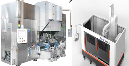
Ensoll’s diamond wire loop addresses each of these requirements through its unique design. The continuous loop configuration enables uninterrupted unidirectional motion, eliminating the wire marks and surface irregularities that can occur with reciprocating wire systems. The diamond abrasive particles are precisely embedded in the wire surface, providing consistent cutting action across the entire length of the loop.
For semiconductor manufacturers, the choice of cutting tool directly affects wafer quality. A high-quality diamond wire loop produces wafers with smoother surfaces, tighter thickness tolerances, and less subsurface damage—all of which translate to higher device yields and lower manufacturing costs.
Step 4: Shaping and Polishing
After slicing, the raw wafer undergoes several finishing steps:
Edge Grinding: The sharp edge of the sliced wafer is rounded to prevent chipping during handling. A notch or flat is also ground into the edge to indicate crystalline orientation, helping subsequent manufacturing equipment align to the wafer.
Lapping: The wafer is pressed between rotating plates with an abrasive slurry to flatten the surfaces and remove saw marks.
Etching: Chemical etchants remove subsurface damage left by slicing and lapping. This step reveals a damage-free surface ready for polishing.
Chemical Mechanical Polishing (CMP): The wafer surface is polished to atomic-level smoothness—essential for photolithography, where circuit patterns are projected onto the wafer with nanometer precision.
Cleaning: Finished wafers are cleaned to remove any particles or chemical residues. A single dust particle can ruin dozens of chips, so cleanliness is paramount.
Step 5: The Finished Fab Wafer
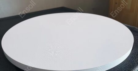
The completed wafer is a masterwork of materials processing. It is perfectly flat, atomically smooth on the front surface, and free of structural defects. The wafer is sealed in protective cassettes and shipped to fabrication facilities, where it will undergo hundreds of additional processing steps to become integrated circuits.
Part Three: The Structure and Characteristics of Fab Wafers
Crystallographic Orientation
The crystal orientation of a silicon wafer is defined by the Miller indices of the surface plane. The two most common orientations are:
– (100) wafers: The surface plane is parallel to one of the cube faces. These wafers have lower interface trap density and are preferred for CMOS (Complementary Metal-Oxide-Semiconductor) devices.
– (111) wafers: The surface plane cuts across the cube diagonally. These wafers have higher atomic density and were common in early bipolar transistor manufacturing.
The orientation affects electrical properties, etching behavior, and mechanical strength. Manufacturers select orientation based on the specific devices being built.
Doping and Resistivity
Pure silicon has relatively high electrical resistance. To make it useful for devices, manufacturers add carefully controlled amounts of dopant atoms—elements with either three or five valence electrons:
– N-type doping: Adding phosphorus or arsenic (five valence electrons) introduces extra free electrons as charge carriers.
– P-type doping: Adding boron (three valence electrons) creates “holes”—missing electrons that act as positive charge carriers.
The concentration of dopants determines the wafer’s resistivity, which must be precisely controlled for the intended device application. High-power devices may require low-resistivity wafers, while high-frequency devices may need higher resistivity.
Wafer Flats and Notches
Every fab wafer has features that help manufacturing equipment orient the wafer correctly. Older wafers use one or more flats—straight edges ground into the circumference. A primary flat indicates crystal orientation, while secondary flats indicate conductivity type and orientation.
Modern 300mm wafers use a single notch—a small indentation at the wafer edge. The notch provides the same orientation information as flats but preserves more usable wafer area.
Surface Quality Specifications
Fab wafers are characterized by several quality metrics:
– TTV (Total Thickness Variation): The difference between maximum and minimum thickness across the wafer.
– Bow: The deviation from flatness across the entire wafer.
– Warp: A more complex measure of overall wafer flatness.
– Surface Roughness (Ra): Typically measured in angstroms (Å) or nanometers.
– Particle Count: The number of microscopic particles on the wafer surface.
These specifications are tightened with each generation of semiconductor technology. For cutting-edge processes, wafers must be virtually perfect.
Part Four: The Role of Fab Wafers in Semiconductor Manufacturing
The Fab Facility
A semiconductor fabrication facility (or “fab”) is one of the most expensive and technologically complex manufacturing environments ever created. A leading-edge fab can cost over $20 billion to build and equip.
The fab maintains a cleanroom environment thousands of times cleaner than a hospital operating room. Air is continuously filtered to remove particles. Workers wear “bunny suits” that cover their entire bodies. Even the materials used in construction are selected to minimize contamination.
The Major Process Steps
Once a fab wafer enters production, it undergoes hundreds of individual process steps, which can be grouped into several categories:
- Oxidation and Deposition
The wafer surface is exposed to high-temperature oxygen or steam, growing a thin layer of silicon dioxide. This oxide serves as an insulator or as a sacrificial layer for subsequent steps. Other materials (silicon nitride, polysilicon, various metals) are deposited using chemical vapor deposition (CVD) or physical vapor deposition (PVD).
- Photolithography
This is the most critical and expensive step in chip manufacturing. A light-sensitive chemical called photoresist is spun onto the wafer surface. Light (typically deep ultraviolet or extreme ultraviolet) shines through a mask—a quartz plate bearing the circuit pattern for one layer. The pattern is projected onto the wafer at reduced size.
Where the light strikes, the photoresist changes chemistry. After developing (washing with a chemical solution), the pattern remains in the photoresist, ready for the next step.
- Etching
The patterned photoresist protects some areas of the wafer while exposing others. Etching removes material from the exposed areas. Plasma etching (dry etching) uses reactive gases energized by radio frequency power to chemically attack the wafer surface. It can create highly anisotropic (directional) features, essential for small geometries.
- Ion Implantation
To create transistor regions with specific electrical properties, dopant atoms must be introduced into precise locations. An ion implanter accelerates dopant ions (boron, phosphorus, arsenic) to high energies and shoots them into the wafer surface. The photoresist pattern from lithography determines where the ions land.
- Deposition and Planarization
After implantation and resist removal, additional layers of material are deposited. The wafer surface becomes increasingly uneven with each layer. Chemical Mechanical Polishing (CMP) flattens the surface, ensuring that subsequent lithography steps can maintain focus across the entire wafer.
- Metallization
The final major step creates the metal wiring that connects transistors. Copper is the most common interconnect material today. Trenches and vias are etched into insulating layers, then filled with copper using electroplating. Excess copper is removed by CMP, leaving only the embedded wiring.
The Multilayer Structure
Modern chips contain 10 to 15 or more metal layers. Each layer requires its own cycle of deposition, lithography, etching, and polishing. The bottom layers (closest to the silicon) handle local connections between nearby transistors. The upper layers are thicker and carry power and signals across longer distances.
After all layers are complete, the wafer is tested while still in its full form. A probe card with hundreds or thousands of microscopic needles contacts bond pads on each chip, testing for electrical function. Bad chips are marked with ink or recorded in a computer file.
Part Five: Applications of Fab Wafers
Microprocessors (CPUs)
The most familiar semiconductor product, microprocessors power computers, servers, and high-end embedded systems. These chips require the most advanced process nodes—currently 3nm and 5nm—and consequently the highest-quality fab wafers. Defects that would be harmless in a memory chip can render a microprocessor completely nonfunctional.
Memory Chips
DRAM (Dynamic Random Access Memory) and NAND Flash are produced in enormous volumes. Memory chips have regular, repetitive structures that can tolerate some defects throughredundancy. Nevertheless, wafer quality directly affects memory yield and cost.
Analog and Power Devices
Not all chips are digital. Analog chips process continuous signals—audio, video, sensor readings. Power devices handle high voltages and currents for power supplies, motor drives, and electric vehicles. These often use larger feature sizes (90nm to 180nm) and may use specialized wafer materials like silicon carbide (SiC) or gallium nitride (GaN).
Sensors and MEMS
Micro-electromechanical systems (MEMS) integrate mechanical structures with electronics. Accelerometers (in smartphones and airbag systems), gyroscopes, microphones, and pressure sensors all start as fab wafers. These devices often require specialized wafer processing, including deep etching to create moving parts.
Optoelectronics
Image sensors (in digital cameras and phones), LEDs, and laser diodes are built on wafers as well. While many of these use gallium arsenide or sapphire substrates rather than silicon, the fundamental wafer-based manufacturing paradigm remains the same.
Part Six: The Critical Enabler—Diamond Wire Loop Cutting Technology
Why Cutting Matters
Throughout this exploration of fab wafers, one truth emerges: the quality of the wafer begins with the cut. A poorly sliced ingot produces wafers with:
– Thickness variations that complicate subsequent processing
– Surface damage that requires excessive polishing (wasting valuable silicon)
– Microscopic cracks that can propagate during thermal cycling
– Rough edges that generate particles during handling
Each of these problems reduces yield, increases cost, or both.
How Diamond Wire Loop Technology Works
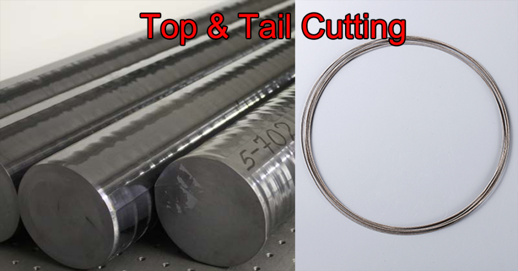
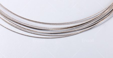
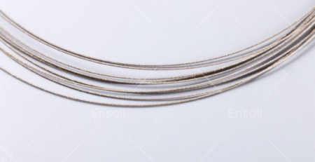
Ensoll’s diamond wire loop represents a significant advancement in precision slicing technology. The system uses a continuous loop of steel wire with diamond abrasive particles embedded in the surface. This loop moves in a single, uninterrupted direction, passing across the crystal ingot to slice wafers..
The continuous loop configuration offers several fundamental advantages for fab wafer production:
- Uninterrupted Motion: Traditional reciprocating wire saws must stop, reverse direction, and re-accelerate thousands of times during a single cut. Each reversal introduces vibration and stress. A continuous diamond wire loop moves constantly in one direction, eliminating these sources of cut variation.
- Consistent Cutting Action: As the diamond wire loop passes through the ingot, fresh diamond abrasive is continuously presented to the cutting zone. This maintains consistent cutting efficiency from start to finish.
- Narrow Kerf: The diamond wire loop is exceptionally thin—diameters down to 0.30mm or less are available. The resulting kerf (the width of material removed) is far narrower than what older saw technologies could achieve. For expensive semiconductor crystals, this reduction in kerf loss directly translates to more wafers per ingot.
- Low Subsurface Damage: Research has shown that the cutting action of a diamond wire involves a combination of plastic deformation and brittle fracture, depending on crystal orientation and cutting parameters. By optimizing these parameters, manufacturers can minimize the depth of subsurface damage, preserving more usable wafer thickness.
Applicability to Advanced Materials
While silicon remains the dominant semiconductor material, the industry increasingly uses other substrates for specialized applications:
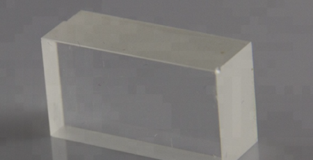
- Silicon Carbide (SiC): Used for high-power, high-frequency, and high-temperature devices. SiC is extremely hard (9.5 on Mohs scale) and challenging to cut. Diamond wire loop technology is essential for slicing SiC ingots into wafers.
- Sapphire (Al₂O₃): Used for LED substrates and specialty electronic applications. Sapphire is also very hard and requires diamond tooling for efficient cutting.
- Gallium Nitride (GaN): Used for RF power amplifiers and high-voltage switching devices. GaN wafers are typically sliced from bulk crystals or grown on foreign substrates.
- Lithium Niobate (LiNbO₃): Used for optical modulators and surface acoustic wave (SAW) filters. This material is piezoelectric and requires careful cutting to preserve its crystalline properties.
In each case, the hardness and brittleness of these advanced materials demand the cutting power of diamond abrasives. A high-quality diamond wire loop provides the precision and consistency that these exacting applications require.
Part Seven: Quality Metrics and Selection Criteria
For Fab Wafer Manufacturers
When selecting a cutting solution for wafer production, manufacturers evaluate several performance metrics:
- Surface Roughness (Ra): The average deviation of the cut surface from ideal flatness. Lower roughness reduces the amount of material that must be removed during subsequent polishing. Research on 12-inch SiC wafers has shown that optimizing cutting parameters can achieve surface roughness below 100nm on certain crystal faces.
- Total Thickness Variation (TTV): The difference between maximum and minimum thickness across the wafer. Lower TTV means the saw produced a more uniform wafer. For 300mm silicon wafers, TTV of just a few microns is typical.
- Subsurface Damage Depth: The thickness of the layer beneath the cut surface that contains cracks or structural alterations. This damaged material must be removed by etching and polishing. Minimizing damage depth preserves wafer thickness and reduces processing costs.
- Kerf Loss: The width of material converted to swarf (cutting debris) during slicing. Lower kerf loss means more wafers from each ingot. For diamond wire cutting, kerf widths as low as 0.35mm are achievable.
- Wire Life: The length of cutting that can be performed before the diamond abrasive wears out. Longer wire life reduces consumable costs and machine downtime.
Conclusion: The Foundation of Modern Electronics
The fab wafer is a remarkable product of materials science and precision engineering. From common sand to a flawless crystalline disk, the journey requires extraordinary control over purity, structure, and geometry. And at the heart of that journey is the cutting process—the moment when a massive crystal ingot becomes thin, flexible wafers ready for chip manufacturing.
**Ensoll’s diamond wire loop technology** represents the modern standard for this critical operation. The continuous loop design enables smooth, consistent cutting with minimal waste and damage. For semiconductor manufacturers demanding ever-higher quality at ever-lower cost, the precision of the diamond wire loop is not merely an advantage—it is a necessity.
The next time you hold a smartphone, start a car, or boot a computer, consider the journey that made it possible. Somewhere along that journey, a crystal ingot was mounted on a precision saw, and a diamond wire loop sliced it into thin wafers—each one a foundation for the integrated circuits that define our world.