
NdFeB 磁石のしくみ, 機能と適用範囲
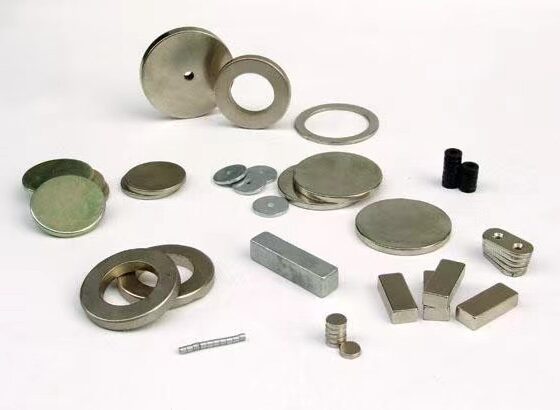
NdFeB 磁石のしくみ, function and application range NdFeB magnets were invented in the early 1980s, そして現在 2009, 利用可能な最強の永久磁石です. 彼らの強み, 小型, 低コストにより、パーソナルオーディオの多くの進歩が可能になりました,…
NdFeB 磁石のしくみ, function and application range NdFeB magnets were invented in the early 1980s, そして現在 2009, 利用可能な最強の永久磁石です. 彼らの強み, 小型, 低コストにより、パーソナルオーディオの多くの進歩が可能になりました,…
Reasons for the popularity of SiC compared to traditional silicon wafers Silicon carbide (SiC) ほとんどの人にとってなじみのない用語です, but it has exploded in popularity in recent years and has become a key third type of semiconductor material…
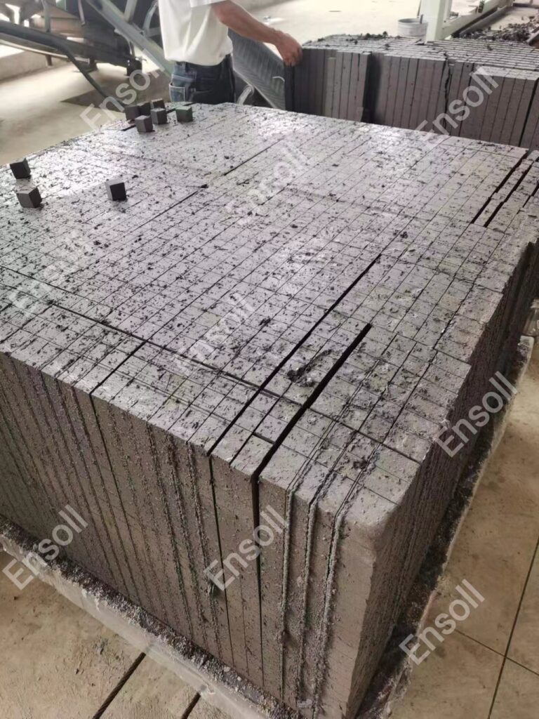
Refractory insulation bricks multi-wire cutting Refractory insulation bricks are refractory raw materials fired from refractory raw materials. 建築窯や各種熱処理設備の高温建材・構造材として使用できます。, and can withstand various…
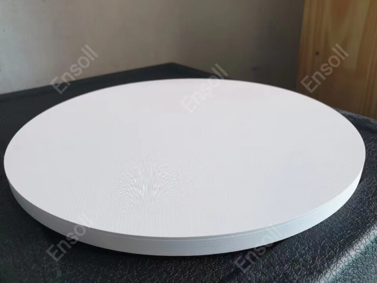
硬さの紹介, classification and cutting of alumina industrial ceramics 1.Introduction to the hardness of alumina industrial ceramic The hardness of alumina industrial ceramic is extremely high. 多結晶アルミナ工業用セラミックスか単結晶アルミナ工業用セラミックスか,…
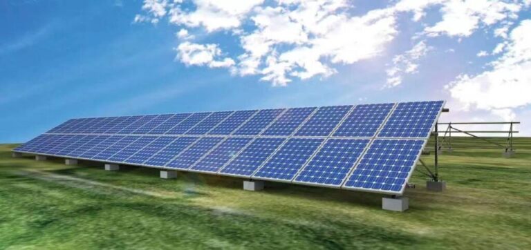
の “高熱” シリコン材料の価格は下がらない, 太陽光発電業界は “前方にロード” “シリコン材料の価格に達しました 310,000 元/トン, そしてそれは 80,000 冒頭の人民元/トン 2021, and there…
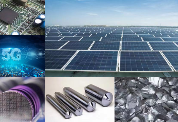
大型半導体ウェーハの需要, manufacturers expand production Fabs are expanding production aggressively, シリコンウェーハの需要は旺盛です. 6月に報告されました 29 それ以上 80% of the production capacity of the 12-inch silicon wafer…
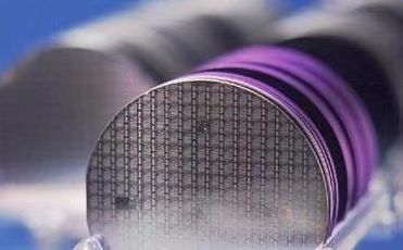
半導体材料 – large-scale silicon wafers Semiconductor materials are divided into wafer fabrication materials and packaging materials. ウェーハ製造材料は、シリコンウェーハとシリコンベースの材料にさらに細分化できます。, フォトマスク, 電子ガス, フォトレジスト, フォトレジストアシスト材料, CMP研磨材,…
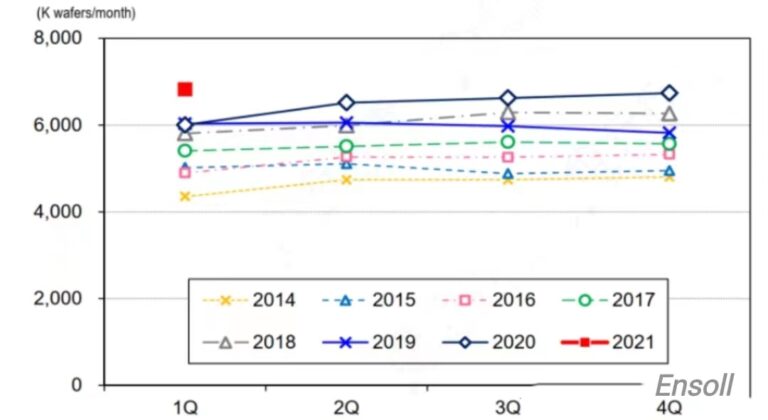
Semiconductor silicon wafer industry analysis In recent years, 半導体市場は、通信インフラの構築により部品の需要が徐々に高まっているため、好調に推移しています。, the continuous increase in the penetration rate of distance education…
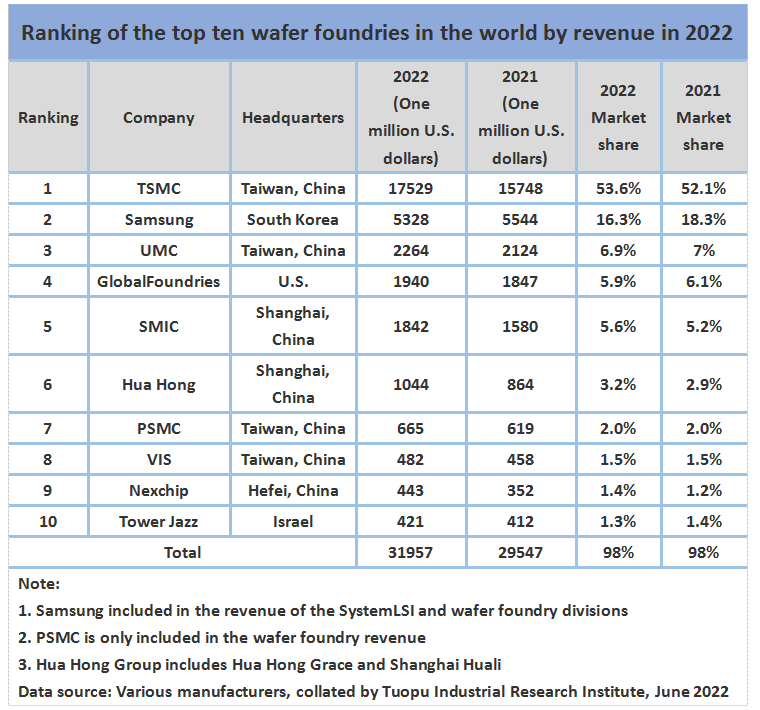
世界のトップ10ウェーハファウンドリの最新ランキング (上 10)! TrendForceの調査によると, 家電製品の需要は引き続き弱いものの, サーバーなどの業界の構造的成長ニーズ, ハイパフォーマンスコンピューティング, automotive and…
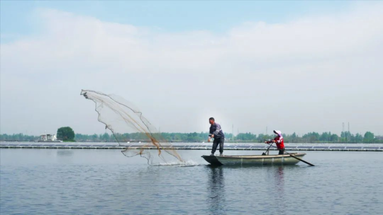
One article to understand the infinite potential of water surface photovoltaic The calm waters carry the sun’s glow, 太陽光発電の新しい機会が生まれています. その高発電で, より少ない土地占有, 有利なエネルギー消費構造の最適化, and the…