
大型半導体ウェーハの需要, メーカーが生産を拡大
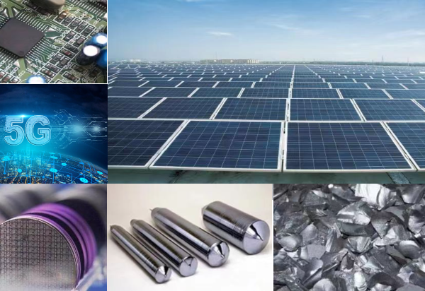
大型半導体ウェーハの需要, manufacturers expand production Fabs are expanding production aggressively, シリコンウェーハの需要は旺盛です. 6月に報告されました 29 それ以上 80% of the production capacity of the 12-inch silicon wafer…
大型半導体ウェーハの需要, manufacturers expand production Fabs are expanding production aggressively, シリコンウェーハの需要は旺盛です. 6月に報告されました 29 それ以上 80% of the production capacity of the 12-inch silicon wafer…
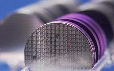
半導体材料 – large-scale silicon wafers Semiconductor materials are divided into wafer fabrication materials and packaging materials. ウェーハ製造材料は、シリコンウェーハとシリコンベースの材料にさらに細分化できます。, フォトマスク, 電子ガス, フォトレジスト, フォトレジストアシスト材料, CMP研磨材,…
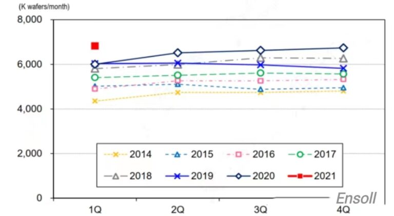
Semiconductor silicon wafer industry analysis In recent years, 半導体市場は、通信インフラの構築により部品の需要が徐々に高まっているため、好調に推移しています。, the continuous increase in the penetration rate of distance education…
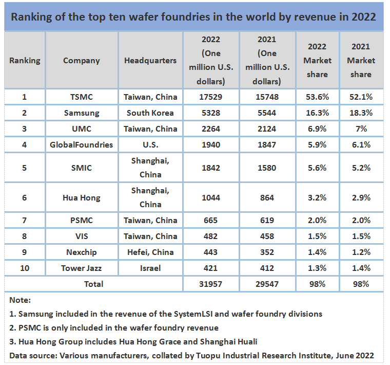
世界のトップ10ウェーハファウンドリの最新ランキング (上 10)! TrendForceの調査によると, 家電製品の需要は引き続き弱いものの, サーバーなどの業界の構造的成長ニーズ, ハイパフォーマンスコンピューティング, automotive and…
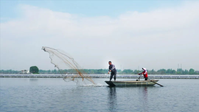
One article to understand the infinite potential of water surface photovoltaic The calm waters carry the sun’s glow, 太陽光発電の新しい機会が生まれています. その高発電で, より少ない土地占有, 有利なエネルギー消費構造の最適化, and the…
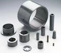
Silicon Carbide Overview Silicon carbide (ママ) は、炭素とシリコンで構成されるIV-V族化合物半導体材料です。, シリコンと炭素を含む硬質化合物. 半導体として, it is extremely rare in nature and occurs in the form of…
1分で石英ガラスを理解する! 石英ガラスは、二酸化ケイ素の単一成分で構成される特殊な工業用技術ガラスです。. 通常のガラスにはない優れた特性を備えています。. It is praised as…
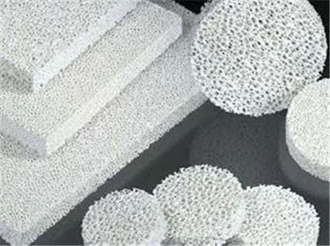
Application of foam ceramics Foam ceramic is a kind of porous material, これは、通常の多孔質セラミックの第1世代とハニカム多孔質セラミックの第2世代に続いて開発された第3世代の多孔質セラミック製品です。. Its pore…
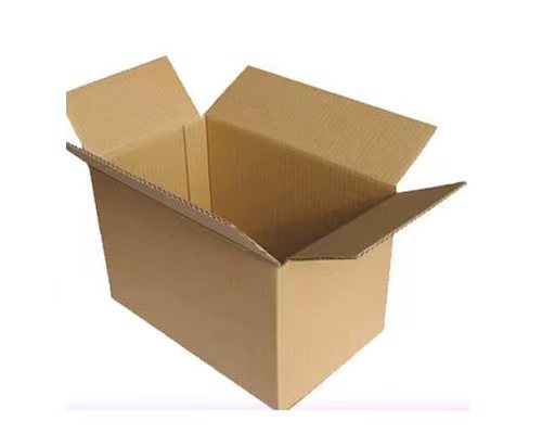
Corrugated paper overview Corrugated paper is a plate-like object formed by bonding liner paper and corrugated corrugated paper formed by corrugating roll processing. 一般的にシングル段ボールとダブル段ボールに分けられます, according to the size of the corrugated…
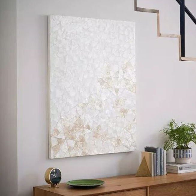
家庭生活自然風 – shell tiles Since ancient times, 貝殻は文化において重要な役割を果たしてきました, 経済と芸術。西洋の伝説では, 金星, 動物や植物の成長と繁殖を担当する愛の神, was…