Gen anpil pwosesis fabrikasyon pou gaufre Silisyòm semi-conducteurs, ak baryè endistri yo wo anpil
The manufacturing process of semiconductor silicon wafers is complex, and single crystal pulling is the key link
The upstream of semiconductor wafers is semiconductor-grade polysilicon material, and the downstream is semiconductor products.
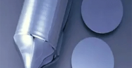
The manufacturing process of semiconductor silicon wafers is complex, mainly including processes such as pulling single crystals and cutting, grinding, polishing and epitaxy of silicon wafers.
The production process of semiconductor silicon wafers is complex and involves many processes. The grinding sheet process includes pulling single crystal, truncating, spheronizing, slicing, chamfering, grinding, elatriye.
The polishing sheet is manufactured on the basis of the grinding sheet through edge polishing, surface polishing and other processes; The silicon annealed sheet is produced by annealing heat treatment, and the silicon-on-insulator SOI is produced by a special process.
Silicon wafers need to be cleaned many times during the manufacturing process, and they also need to be inspected and packaged before being sold to customers.
The semiconductor silicon wafer industry has high barriers, and the first-mover advantage and scale effect are prominent
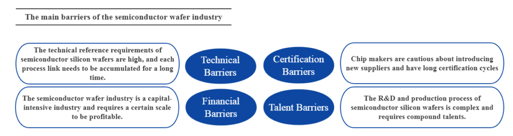
Technical barriers: The technical parameters of semiconductor silicon wafers are highly required, and each process link needs to be accumulated for a long time.
The core processes of semiconductor silicon wafers include single crystal process, slicing process, grinding process, polishing process, epitaxy process, elatriye. The technology has a high degree of specialization.
Pami yo, the single crystal process is the most core technology, which determines the size, resistivity, Key technical indicators such as purity, oxygen content, dislocation, crystal defects, elatriye., need to pay attention to temperature control and pulling rate in the process of single crystal growth.
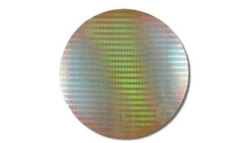
Wafer grinding and polishing processes determine the thickness, sifas plat, surface cleanliness, surface granularity, warpage and other indicators of the silicon wafer. The focus of the epitaxial process is to ensure the uniformity of the thickness of the epitaxial layer and the intra-chip uniformity of the resistivity of the epitaxial layer.
Barriers to customer certification: Chip manufacturers are cautious about introducing new suppliers and have long certification cycles. Semiconductor silicon wafers are an important raw material for chip manufacturers to produce semiconductor products.
Chip manufacturers are cautious about introducing new suppliers. In order to ensure the stability and consistency of product quality, a long certification cycle is required. Anjeneral, chip manufacturing companies will require silicon wafer suppliers to provide some silicon wafers for their trial production.
After passing internal certification, the chip manufacturing company will send the products to downstream customers and obtain the approval of their customers. The supplier is certified, and finally the procurement contract is formally signed.
Capital barriers and scale barriers: The semiconductor silicon wafers industry is a capital-intensive industry and requires a certain sales scale to be profitable. Pwodiksyon gwo-echèl nan gauf Silisyòm semi-conducteurs mande pou yon gwo kantite envestisman.
Pa egzanp, a key production equipment is worth tens of millions of yuan, and the investment amount of a large-scale silicon wafer production line is one billion yuan. An menm tan, due to the large amount of investment in fixed assets in the early stage, konpayi wafer semiconductor bezwen fòme yon sèten echèl nan lavant yo anvan yo ka fè pwofi.
Presyon an opere nan etap nan bonè se relativman gwo, ak to pwofi brit la ka negatif.
Talent barriers: Semiconductor silicon wafers companies need compound talents. The R&D and production process of semiconductor silicon wafers is relatively complex, involving the intersection of solid state physics, quantum mechanics, thermodynamics, chemistry and other multidisciplinary fields.
Se poutèt sa, compound talents with comprehensive professional knowledge and rich production experience are required.
https://www.youtube.com/watch?v=N57A-9mi-Mk
Kontakte nou pou konnen plis !
ak isit la yo aplikasyon ki pi enteresan .