Rapport de recherche spécial sur l'industrie du carbure de silicium: croissance des véhicules à énergies nouvelles et de l'industrie des moteurs photovoltaïques(1)
1. SiC has excellent electrical characteristics and is expected to become one of the most promising semiconductor materials
The development of semiconductor materials has gone through three stages. Les matériaux semi-conducteurs courants incluent le silicium (Et), germanium (Ge) et d'autres éléments semi-conducteurs et matériaux semi-conducteurs composés tels que l'arséniure de gallium (AsGa), carbure de silicium (SiC), nitrure de gallium (GaN). De la séquence temporelle de la recherche et de l'application à grande échelle, the above semiconductor materials are generally divided into three generations in the industry.
The first generation semiconductor materials have been widely used since the 1950s, représenté par le silicium (Et) and germanium (Ge). The industrial chain of such materials is relatively mature, with complete technical reserves and low production costs. Maintenant, they are mainly used in large-scale integrated circuits, including low-voltage, low-frequency, low-power transistors and detectors.
Silicon based semiconductor materials are currently the largest output and most widely used semiconductor materials, et plus que 90% of semiconductor products are made of silicon based materials.
The second generation semiconductor materials have been widely used since the 1990s, représenté par l'arséniure de gallium (AsGa) and indium phosphide (InP). With the development of semiconductor industry, the physical bottleneck of silicon material is increasingly emerging, and its physical properties limit its application in optoelectronics and high-frequency high power devices. The second generation semiconductor materials have the characteristics of direct band gap in physical structure.
Compared with silicon based materials, they have the advantages of good photoelectric performance, high operating frequency, high temperature resistance and radiation resistance. They are suitable for making high-speed, haute fréquence, high-power and light-emitting electronic devices. They are excellent materials for making high-performance microwave, millimeter wave devices and light-emitting devices, and are widely used in mobile communications, communication par satellite, optical communications, GPS navigation and other fields.
The third generation semiconductor is a compound semiconductor represented by gallium nitride (GaN) and silicon carbide (SiC). The band gap width of this type of semiconductor material is greater than or equal to 2.3eV, so it is also called wide band gap semiconductor material. The third generation semiconductor has significant advantages in key parameters such as band gap width, breakdown electric field, thermal conductivity, electronic saturation rate, and radiation resistance, meeting the needs of modern industry for high power, high voltage, and high frequency.
Donc, the third generation semiconductor is mainly used to make high-speed, haute fréquence, high-power and light-emitting electronic components. Downstream applications include smart grid, véhicules à énergies nouvelles, photovoltaic wind power, 5G communication, etc..
Introduction to SiC materials. SiC is an inorganic substance with the chemical formula of SiC. It is made of quartz sand, petroleum coke (or coal coke), wood chips (salt is needed to produce green SiC) and other raw materials by smelting in a resistance furnace at high temperature.
SiC also exists in nature as a rare mineral, mullite. Among C, Nouvelles, B and other non oxide high-tech refractory materials, SiC is the most widely used and economical one, which can be called emery or refractory sand. SiC is expected to become one of the most promising materials in the field of semiconductor materials.
Compared with silicon devices, power devices based on SiC have electrical properties such as high voltage resistance, high temperature resistance and low energy loss, and are one of the most promising semiconductor materials. The superior electrical characteristics of SiC include the following aspects:
1 High voltage resistance. As the breakdown electric field strength of SiC is more than 10 times that of silicon, the device prepared with SiC can further improve the withstand voltage capacity, operating frequency and current density, and significantly reduce the conduction loss of the device.
2 Résistance aux hautes températures. The wider the band gap is, the higher the limiting operating temperature of the device will be. Since the band gap of SiC is close to three times of that of silicon, the limiting operating temperature of SiC will be significantly higher than that of silicon, which can reach more than 600 ℃. En même temps, the thermal conductivity of SiC is higher than that of silicon, which helps to reduce the requirements for the cooling system and make the terminal lighter and smaller.
3 Low energy loss. SiC has a saturated electron drift rate twice that of silicon. Compared with silicon, SiC has a very low on resistance and low on loss; En même temps, SiC has nearly 3 times the band gap width of silicon, and the leakage current is significantly reduced compared with silicon devices, which can further reduce the power loss; En outre, SiC devices do not have current tailing during the turn off process, and the switching loss is low, which greatly improves the switching frequency in practical applications.
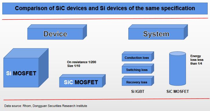
En général, SiC has superior properties such as high pressure resistance, high temperature resistance and low energy loss, which can meet the new requirements of power electronics technology for high temperature, high power, high voltage, haute fréquence, radiation resistance and other harsh working conditions, and is expected to become one of the most promising materials in the field of semiconductor materials.