
Pooljuhtmaterjalid – suuremahulised räniplaadid
Semiconductor materials are divided into wafer fabrication materials and packaging materials. Vahvlite valmistamise materjale saab veelgi jagada ränivahvliteks ja ränipõhisteks materjalideks, fotomaskid, elektrongaasid, fotoresistid, fotoresist abimaterjalid, CMP poleerimismaterjalid, töödelda kemikaale, sihtmärgid, and other materials.
The packaging materials can be further subdivided into packaging substrates, lead frames, bonding wires, encapsulation materials, ceramic substrates, die attach materials and other packaging materials.
Overall, the market segment of semiconductor materials is scattered and small in scale. Only silicon wafers account for nearly 35% of the market share. Silicon wafers occupy the absolute mainstream of the semiconductor material market, followed by electronic gases accounting for 13%, photomasks accounting for 12%.
The remaining photoresist supporting chemicals, polishing materials, photoresist, wet chemicals, sputtering targets and other materials account for less than 10%, and the scale is relatively small.
The third generation of semiconductors: wide-bandgap semiconductor materials represented by gallium nitride (GaN), ränikarbiid (SiC), and zinc oxide (ZnO). It has excellent properties such as high breakdown electric field, kõrge soojusjuhtivus, high electron saturation rate and strong radiation resistance, and is more suitable for making high-temperature, high-frequency, radiation-resistant and high-power electronic devices.
It has broad application prospects in semiconductor lighting, new generation mobile communications, energy Internet, high-speed rail transit, uued energiasõidukid, consumer electronics and other fields.
The fourth generation of semiconductors: ultra-wide band gap semiconductor materials represented by gallium oxide (Ga2O3), diamond (C), aluminum nitride (AlN), and ultra-narrow band gap semiconductor materials represented by antimonide (GaSb, InSb) .
Ultra-wide band gap materials have more prominent characteristic advantages in the field of high-frequency power devices due to their wider band gaps than third-generation semiconductor materials; Ultra-narrow band gap materials are mainly used in detectors, lasers and other devices due to their easy excitation and high mobility.
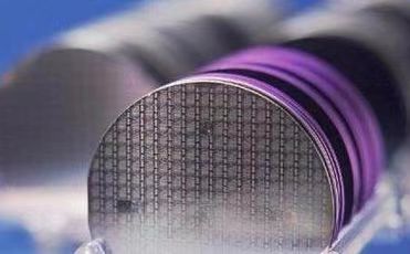
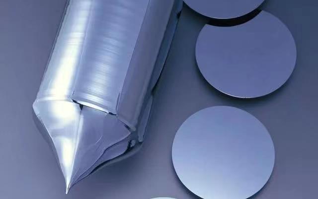
Semiconductor Silicon Wafer is the basis for manufacturing silicon semiconductor products and can be classified according to different parameters.
According to the size (läbimõõt), pooljuht-ränivahvlid saab jagada 2 tolli (50mm), 3 tolli (75mm), 4 tolli (100mm), 5 tolli (125mm), 6 tolli (150mm), 8 tolli (200mm), 12 tolli(300mm).
Under the influence of Moore’s Law, semiconductor silicon wafers are constantly developing in the direction of large size. Hetkel, 8-inch and 12-inch are mainstream products, moodustades rohkem kui 90% of the total shipment area.
According to the degree of doping, semiconductor silicon wafers can be divided into lightly doped and heavily doped. Heavy-doped silicon wafers have a large amount of doping elements and low resistivity, and are generally used in power devices and other products;
Lightly doped silicon wafers have low doping concentration and are generally used in the field of integrated circuits, with higher technical difficulty and product quality requirements. Since integrated circuits account for more than 80% of the global semiconductor market, there is a greater global demand for lightly doped silicon wafers.
According to the process, semiconductor silicon wafers can be divided into grinding wafers, polishing wafers, special wafer epitaxial wafers based on polishing wafers, SOI, jne.
Grinding sheets can be used to manufacture discrete devices; lightly doped polishing sheets can be used to manufacture large scale integrated circuits or as substrate materials for epitaxial wafers, and heavily doped polishing sheets are generally used as substrate materials for epitaxial wafers. Compared with abrasive sheets, polishing sheets have better surface flatness and cleanliness.
The semiconductor wafer industry is also a capital-intensive industry, which needs to reach a certain sales scale to be profitable: Pooljuht-räniplaatide suuremahuline tootmine nõuab suuri investeeringuid.
Due to the large investment in fixed assets in the early stage, pooljuhtplaatide ettevõtted peavad enne kasumi teenimist moodustama teatud müügimahu. Töörõhk varases staadiumis on suhteliselt suur, ja brutokasumi määr võib olla negatiivne.
Hetkel, the use of silicon wafers by downstream chip companies: diskreetsed seadmed kasutavad jätkuvalt väikeseid suurusi, ja integraallülitused migreeruvad suurtele suurustele.
Diskreetsete seadmete madala hinna tõttu, tootjad ei ole motiveeritud investeerima suuremahulistesse tootmisliinidesse. Hetkel, räniplaadid 6 tolli ja alla selle on endiselt peamised tooted.
Suuremõõtmeliste räniplaatide integraallülitustes kasutamisest saadav majanduslik kasu on ilmne.
Näiteks, 12-tollise räniplaadi pindala on 2.25 korda võrreldes 8-tollise vahvliga, ja kasutatav määr on umbes 2.5 korda võrreldes 8-tollise vahvliga. The number of chips that can be produced on a single chip increases, and the cost of a single chip decreases.
Driven by new demands such as telecommuting, veebikohtumised, autonoomne sõit, ja metaversum, the demand for 12-inch semiconductor silicon wafers will continue to increase.
