Fitaovana semiconductor – wafers silisiôma lehibe
Semiconductor materials are divided into wafer fabrication materials and packaging materials. Ny fitaovam-pamokarana wafer dia azo zaraina bebe kokoa ho wafers silisiôma sy akora mifototra amin'ny silisiôma, photomasks, gazy elektronika, photoresists, fitaovana fanampiana photoresist, CMP poloney fitaovana, simika fanodinana, lasibatra, ary fitaovana hafa.
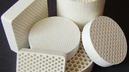
Ny fitaovana famonosana dia azo zaraina amin'ny substrate fonosana, firaka, tariby mifamatotra, fitaovana encapsulation, substrates seramika, die attach fitaovana sy fitaovana hafa fonosana.
ankapobeny, the market segment of semiconductor materials is scattered and small in scale. Only silicon wafers account for nearly 35% of the market share. Silicon wafers occupy the absolute mainstream of the semiconductor material market, followed by electronic gases accounting for 13%, photomasks accounting for 12%.
The remaining photoresist supporting chemicals, fitaovana fanosotra, photoresist, wet chemicals, sputtering targets and other materials account for less than 10%, and the scale is relatively small.
Ny taranaka fahatelo ny semiconductor: fitaovana semiconductor wide-bandgap aseho amin'ny gallium nitride (GaN), silisiôma carbide (sento), ary zinc oxide (ZnO). Manana toetra tena tsara izy io toy ny saha elektrika avo lenta, conductivity mafana mafana, ny tahan'ny saturation elektronika avo sy ny fanoherana taratra mahery vaika, and is more suitable for making high-temperature, avo-hatetika, radiation-resistant and high-power electronic devices.
It has broad application prospects in semiconductor lighting, new generation mobile communications, energy Internet, fiarandalamby haingam-pandeha, fiara angovo vaovao, elektronika mpanjifa sy sehatra hafa.
The fourth generation of semiconductors: fitaovana semiconductor gap midadasika midadasika aseho amin'ny galium oxide (Ga2O3), Diamond (C), aluminium nitride (AlN), and ultra-narrow band gap semiconductor materials represented by antimonide (GaSb, InSb) .
Ny fitaovana hantsana amin'ny tarika ultra-wide dia manana tombony miavaka kokoa amin'ny sehatry ny fitaovana herinaratra avo lenta noho ny elanelan'ny tarika lehibe kokoa noho ny fitaovana semiconductor andiany fahatelo.; Ultra-narrow band gap materials are mainly used in detectors, lasers and other devices due to their easy excitation and high mobility.
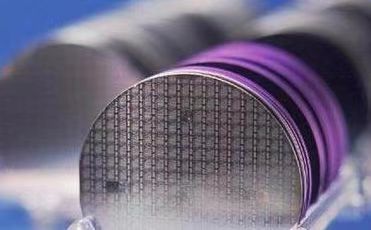
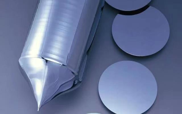
Semiconductor Silicon Wafer is the basis for manufacturing silicon semiconductor products and can be classified according to different parameters.
Araka ny habeny (savaivony), semiconductor silicone wafers azo zaraina ho 2 santimetatra (50MG), 3 santimetatra (75MG), 4 santimetatra (100MG), 5 santimetatra (125MG), 6 santimetatra (150MG), 8 santimetatra (200MG), 12 santimetatra(300MG).
Under the influence of Moore’s Law, semiconductor silicon wafers are constantly developing in the direction of large size. Amin'izao, 8-inch and 12-inch are mainstream products, kaonty mihoatra ny 90% of the total shipment area.
According to the degree of doping, semiconductor silicon wafers can be divided into lightly doped and heavily doped. Heavy-doped silicon wafers have a large amount of doping elements and low resistivity, and are generally used in power devices and other products;
Lightly doped silicon wafers have low doping concentration and are generally used in the field of integrated circuits, with higher technical difficulty and product quality requirements. Since integrated circuits account for more than 80% of the global semiconductor market, there is a greater global demand for lightly doped silicon wafers.
According to the process, semiconductor silicon wafers can be divided into grinding wafers, polishing wafers, special wafer epitaxial wafers based on polishing wafers, SOI, sns.
Grinding sheets can be used to manufacture discrete devices; lightly doped polishing sheets can be used to manufacture large scale integrated circuits or as substrate materials for epitaxial wafers, and heavily doped polishing sheets are generally used as substrate materials for epitaxial wafers. Compared with abrasive sheets, polishing sheets have better surface flatness and cleanliness.
The semiconductor wafer industry is also a capital-intensive industry, which needs to reach a certain sales scale to be profitable: Large-scale production of semiconductor silicon wafers requires a large investment amount.
Due to the large investment in fixed assets in the early stage, semiconductor wafer companies need to form a certain scale of sales before they can make profits. The operating pressure in the early stage is relatively large, and the gross profit rate may be negative.
Amin'izao, the use of silicon wafers by downstream chip companies: mbola mampiasa habe kely ny fitaovana discrete, ary ny circuit integrated dia mifindra any amin'ny habe lehibe.
Noho ny vidiny ambany ny fitaovana discrete, ny mpanamboatra dia tsy voatosika hampiasa vola amin'ny tsipika famokarana lehibe. Amin'izao, silicone wafers ny 6 santimetatra sy ambany no tena vokatra.
Ny tombony ara-toekarena entin'ny fampiasana wafers silisiôma lehibe amin'ny circuit integrated dia miharihary.
Ohatra, Ny velaran'ny wafer silisiôma 12 santimetatra dia 2.25 avo roa heny noho ny wafer 8 santimetatra, ary ny tahan'ny azo ampiasaina dia eo ho eo 2.5 avo roa heny noho ny wafer 8 santimetatra. The number of chips that can be produced on a single chip increases, and the cost of a single chip decreases.
Driven by new demands such as telecommuting, fivoriana an-tserasera, mitondra fiara tsy miankina, ary ny Metaverse, the demand for 12-inch semiconductor silicon wafers will continue to increase.