giu
First analyze the classification and application scope of silicon wafers, giu.
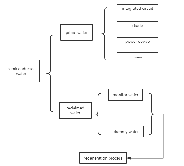
giu, i wafer di silicio possono essere suddivisi in Dummy Wafer, Monitor Wafer e Prime Wafer.
Tra loro, Il Dummy Wafer e il Monitor Wafer sono generalmente tagliati dalla scarsa qualità su entrambi i lati del lingotto di silicio, which are used to debug the machine and monitor the yield.
With the advancement of the fab process, based on the accuracy requirements and yield considerations, it is necessary to increase the monitoring frequency during the production process.
For every 10 pieces of Prime Wafer in the 65nm process, 6 pieces of Dummy Wafer and Monitor Wafer need to be added.
For 28nm and below process, every 10 pieces of Prime Wafer need to add 15-20 pieces of Dummy Wafer and Monitor Wafer.
The amount of Dummy Wafer and Monitor Wafer is huge. In order to avoid waste, the fab often recycles the used Dummy Wafer, grinds and polishes it, and reuses it.
tuttavia, the number of cycles of Dummy Wafer is limited. Once the threshold value is exceeded, it can only be scrapped or used as a photovoltaic silicon wafer.
Monitor Wafer needs to be treated on a case-by-case basis. Monitor Wafer used in some special processes cannot be recycled. Those Dummy Wafer and Monitor Wafer that can be recycled and reused are also called reclaimed wafers.
Semiconductor silicon wafers can be divided according to size, process, e simili. Secondo le dimensioni, it can be generally divided into 12 pollici (300mm), 8 pollici (200mm), 6 pollici (150mm), 5 pollici (125mm), 4 pollici (100mm) and other specifications.
The upgrade of advanced chip processes is an important driving factor for the development of the semiconductor industry, and breakthroughs in the process have brought about an increase in the demand for supporting semiconductor equipment and materials.
The development of advanced technologies in consumer electronics, elettronica automobilistica, computers and other application fields such as 5G, artificial intelligence, smart transportation, eccetera., puts forward higher requirements for chip performance and promotes the upgrade of chip manufacturing processes.
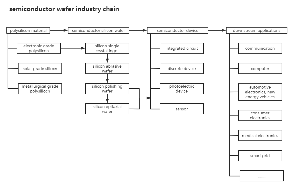
Regarding the scope of application of silicon wafers, we can analyze from the industrial chain. The upstream of the semiconductor silicon wafer industry chain is polysilicon, aprile. aprile, aprile,
aprile. aprile.
Perciò, silicon wafer manufacturers need to meet the long quality verification period of the fab before they can form a stable cooperative relationship. After the silicon wafer is processed into semiconductor devices, it is supplied to the terminal application field.
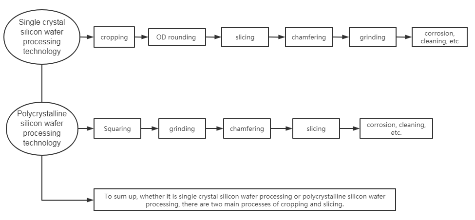
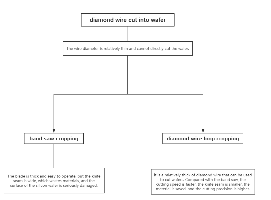
The processing technology of silicon wafer manufacturers is also very important. In the last article, we analyzed the processing technology of silicon wafers and brought annular diamond wires to the public eye.
This article analyzes the classification and application scope of silicon wafers, and illustrates the importance of silicon wafers and the wide range of silicon wafer applications.
Through the figure below, we can find the use of the new technology diamond wire loop.
https://www.youtube.com/watch?v=8CmBm6b3Mgw
Contattaci per saperne di più !
e qui ci sono applicazioni più interessanti .