Halvledermaterialer – storskala silicium wafers
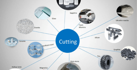
Semiconductor materials are divided into wafer fabrication materials and packaging materials. Waferfremstillingsmaterialer kan yderligere opdeles i siliciumwafers og siliciumbaserede materialer, fotomasker, elektrongasser, fotoresists, fotoresist hjælpematerialer, CMP poleringsmaterialer, proceskemikalier, mål, og andre materialer.
Emballagematerialerne kan yderligere opdeles i emballagesubstrater, blyrammer, bindingstråde, indkapslingsmaterialer, keramiske underlag, matrice vedhæfte materialer og andre emballagematerialer.
samlet set, the market segment of semiconductor materials is scattered and small in scale. Only silicon wafers account for nearly 35% of the market share. Silicon wafers occupy the absolute mainstream of the semiconductor material market, followed by electronic gases accounting for 13%, photomasks accounting for 12%.
The remaining photoresist supporting chemicals, polishing materials, photoresist, wet chemicals, sputtering targets and other materials account for less than 10%, and the scale is relatively small.
Tredje generation af halvledere: halvledermaterialer med bred båndgab repræsenteret ved galliumnitrid (GaN), siliciumcarbid (SiC), og zinkoxid (ZnO). Det har fremragende egenskaber såsom højt nedbrydning elektrisk felt, høj varmeledningsevne, høj elektronmætning og stærk strålingsmodstand, and is more suitable for making high-temperature, høj frekvens, radiation-resistant and high-power electronic devices.
It has broad application prospects in semiconductor lighting, new generation mobile communications, energy Internet, højhastighedstogtransit, nye energikøretøjer, forbrugerelektronik og andre områder.
The fourth generation of semiconductors: halvledermaterialer med ultrabredt båndgab repræsenteret ved galliumoxid (Ga2O3), diamant (C), aluminum nitride (AlN), and ultra-narrow band gap semiconductor materials represented by antimonide (GaSb, InSb) .
Materialer med ultrabredt båndgab har mere fremtrædende karakteristiske fordele inden for højfrekvente strømenheder på grund af deres bredere båndgab end tredje generations halvledermaterialer; Ultra-narrow band gap materials are mainly used in detectors, lasers and other devices due to their easy excitation and high mobility.
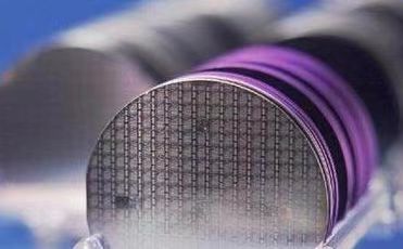
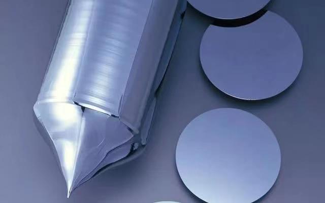
Semiconductor Silicon Wafer is the basis for manufacturing silicon semiconductor products and can be classified according to different parameters.
According to the size (diameter), halvleder silicium wafers kan opdeles i 2 tommer (50mm), 3 tommer (75mm), 4 tommer (100mm), 5 tommer (125mm), 6 tommer (150mm), 8 tommer (200mm), 12 tommer(300mm).
Under the influence of Moore’s Law, semiconductor silicon wafers are constantly developing in the direction of large size. På nuværende tidspunkt, 8-inch and 12-inch are mainstream products, accounting for more than 90% of the total shipment area.
According to the degree of doping, semiconductor silicon wafers can be divided into lightly doped and heavily doped. Heavy-doped silicon wafers have a large amount of doping elements and low resistivity, and are generally used in power devices and other products;
Lightly doped silicon wafers have low doping concentration and are generally used in the field of integrated circuits, with higher technical difficulty and product quality requirements. Since integrated circuits account for more than 80% of the global semiconductor market, there is a greater global demand for lightly doped silicon wafers.
According to the process, semiconductor silicon wafers can be divided into grinding wafers, polishing wafers, special wafer epitaxial wafers based on polishing wafers, SOI, etc.
Grinding sheets can be used to manufacture discrete devices; lightly doped polishing sheets can be used to manufacture large scale integrated circuits or as substrate materials for epitaxial wafers, and heavily doped polishing sheets are generally used as substrate materials for epitaxial wafers. Compared with abrasive sheets, polishing sheets have better surface flatness and cleanliness.
The semiconductor wafer industry is also a capital-intensive industry, which needs to reach a certain sales scale to be profitable: Storskalaproduktion af halvledersiliciumwafers kræver et stort investeringsbeløb.
Due to the large investment in fixed assets in the early stage, halvlederwafervirksomheder skal danne en vis salgsskala, før de kan tjene penge. Driftspresset i den tidlige fase er relativt stort, og bruttoavancen kan være negativ.
På nuværende tidspunkt, the use of silicon wafers by downstream chip companies: diskrete enheder fortsætter med at bruge små størrelser, og integrerede kredsløb migrerer til store størrelser.
På grund af den lave pris på diskrete enheder, producenter er ikke motiverede til at investere i store produktionslinjer. På nuværende tidspunkt, silicium wafers af 6 tommer og derunder er stadig hovedprodukterne.
De økonomiske fordele ved brugen af store siliciumwafers i integrerede kredsløb er indlysende.
For eksempel, arealet af en 12-tommer silicium wafer er 2.25 gange så stor som en 8-tommers wafer, og den brugbare rate er ca 2.5 gange så stor som en 8-tommers wafer. The number of chips that can be produced on a single chip increases, and the cost of a single chip decreases.
Driven by new demands such as telecommuting, online møder, autonom kørsel, og Metaverset, the demand for 12-inch semiconductor silicon wafers will continue to increase.